

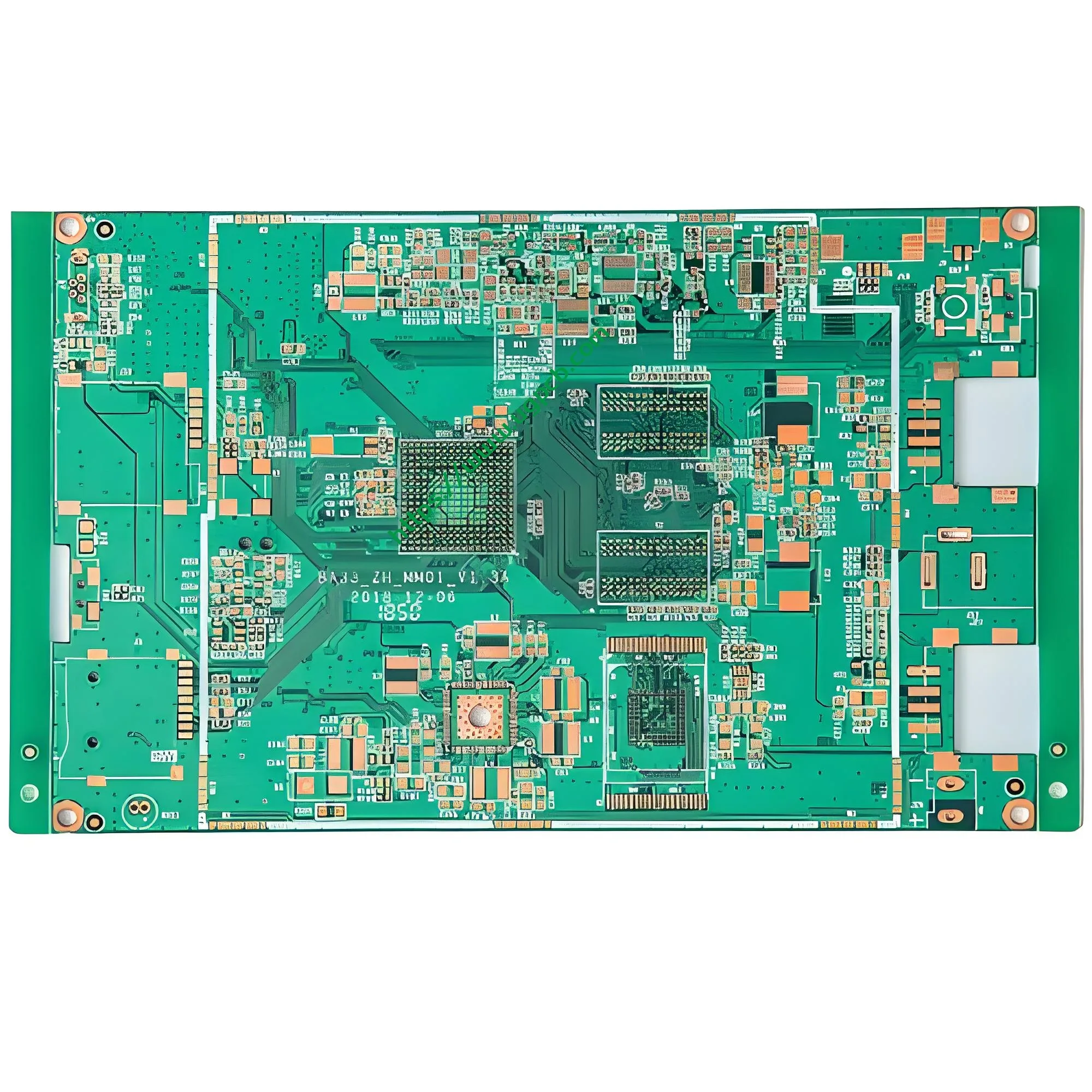
Descripción general del producto: ¿Qué es una placa de circuito PCB antioxidante OSP??
UnPlaca de circuito PCB antioxidante OSP usosConservantes de soldadura orgánica (OSP) como su acabado superficial de cobre. Este proceso deposita una película orgánica ultrafina sobre superficies de cobre desnudas.. La película evita la oxidación durante el almacenamiento y el montaje.. Durante la soldadura, el fundente disuelve rápidamente la película OSP. Esto expone cobre limpio para uniones de soldadura confiables..
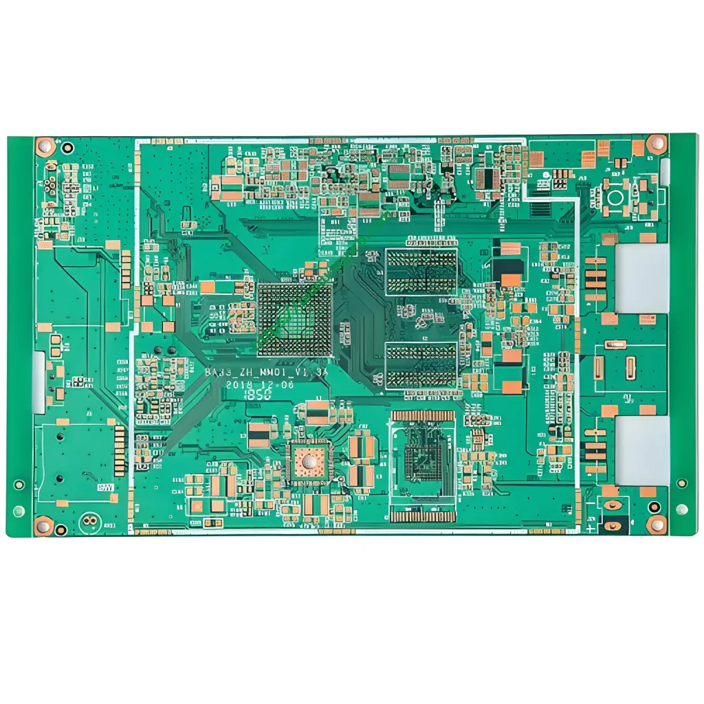
Usos de la placa de circuito PCB antioxidante OSP de UGPCBLaminado epoxi de vidrio FR-4 como material base. Cuenta con 35μm (1 onz) lámina de cobre, 1.6mm de espesor del tablero, y dimensiones de 68.36 × 34,6 mm. El tamaño mínimo del orificio terminado es de 0,45 mm.. El ancho mínimo de la traza es de 0,15 mm y el espacio mínimo es de 0,20 mm. El producto cumple totalmente con IPC-6012E (Calificación y rendimiento del tablero impreso rígido.) y IPC-4555 (rendimiento OSP de alta temperatura) presupuesto.
EstePCB OSP de doble cara sirve electrónica de consumo, equipo de comunicacion, y controles industriales. Funciona mejor donde la sensibilidad al costo y la planitud de la superficie son más importantes.
Clasificación científica de productos
Basado en sistemas internacionales de clasificación de PCB, este producto cae en estas categorías:
| Dimensión de clasificación | Categoría |
|---|---|
| Material de sustrato | PCB rígido de tela de vidrio epoxi FR-4 |
| Número de capas | De dos caras (circuito de dos capas) |
| Acabado superficial | OSP (Conservantes de soldadura orgánica) antioxidante |
| Calificación de inflamabilidad | UL 94 V-0 |
| Clase de rendimiento IPC | Clase 2 (productos electrónicos de servicio dedicado) |
| Espesor de lámina de cobre | 1 onz (35μm) cobre estándar |
| Grosor del tablero | 1.6tablero rígido estándar mm |
| Tipo de agujero | Orificio pasante compatible con SMT |
Parámetros técnicos clave explicados
sustrato: Tela de vidrio epoxi FR-4
FR-4 es el sustrato rígido más común en el tarjeta de circuito impreso industria. “FR” significa retardante de llama. “4” indica resina epoxi combinada con tejido de vidrio que cumpleUL 94 V-0 estándares de inflamabilidad. UL 94 V-0 requiere que las muestras verticales se autoextingan dentro10 artículos de segunda clase después de dos aplicaciones de llama de 10 segundos. Ninguna gota de fuego puede encender el algodón..

La temperatura de transición vítrea (tg) mide la resistencia al calor. El FR-4 Tg estándar oscila entre 130 y 140 °C. El FR-4 de Tg media alcanza 150–160 °C. El FR-4 de alta Tg supera los 170 °C. Este producto utiliza el estándar FR-4 con Tg ≥ 130°C (Cumple con IPC-4101/21). Esto cumple con las demandas de choque térmico de la soldadura por reflujo. (temperaturas máximas 240–260°C).
Espesor de lámina de cobre: 35μm (1 onz)
El espesor del cobre determina la capacidad de transporte de corriente.. Este producto utiliza35μm lámina de cobre, conocido como1 onzas de cobre (1 oz/pie² ≈ 35μm). Según IPC-2221, 1 oz de cobre con un aumento de temperatura de 10°C transporta aproximadamente:
- 0.15milímetros (6 mil) ancho de rastreo: 0.5-0.7A
- 0.20milímetros (8 mil) ancho de rastreo: 0.8-1.0A
El espesor de cobre de 35 μm es el estándar más común para PCB de doble cara.. Equilibra el costo, capacidad actual, y rendimiento de fabricación.
Dimensiones del tablero: 68.36 × 34,6 mm
El tablero terminado mide68.36mm × 34,6 mm. Este tamaño compacto se adapta a módulos electrónicos estrechos.. Los PCB pequeños exigen una mayor precisión: las tolerancias dimensionales normalmente se mantienen dentro de ±0,15 mm. (Clase IPC-6012 2).
Tamaño mínimo del orificio terminado: 0.45milímetros
0.45milímetros es el orificio pasante mínimo chapado (PTH) diámetro. Este tamaño de orificio es un estándar en la industria.. Garantiza un revestimiento fiable (relación de aspecto aproximadamente 3.6:1 con tablero de 1,6 mm de espesor). El tamaño del orificio se adapta a la mayoría de los componentes DIP y diseños de almohadillas SMT estándar..
Grosor de la placa de circuito impreso: 1.6milímetros
1.6milímetros es el espesor de placa más común en la fabricación de PCB. Proporciona una excelente resistencia mecánica y rigidez a la flexión.. Combina perfectamente con conectores y enchufes estándar.
Trace ancho y espaciado: 0.15milímetros / 0.20milímetros
Este producto ofreceancho mínimo de traza de 0,15 mm (acerca de 6 mils) yespacio mínimo de 0,20 mm (acerca de 8 mils). Según clasificación IPC, estas dimensiones caen enClase 2 (productos electrónicos de servicio dedicado). Esta precisión cumple con la mayoría de los diseños de PCB de densidad media., incluyendo tableros de control MCU, módulos de administración de energía, y placas convertidoras de interfaz.
Cómo funciona el proceso antioxidante OSP
El proceso OSP genera una película orgánica ultrafina sobre cobre limpio y desnudo a través deadsorción química. La película OSP se compone principalmente decompuestos de alquilbencimidazol (a base de azol). El espesor de la película suele oscilar entre0.2–0,5 µm.
Mecanismo de protección
La película OSP protege las superficies de cobre mediante tres mecanismos.:
- Barrera física – La película orgánica forma una densa capa molecular.. Bloquea el contacto del oxígeno y la humedad con la superficie de cobre..
- Adsorción química – Los grupos activos en las moléculas de OSP se unen químicamente con átomos de cobre.. Esto crea una fuerte adhesión..
- Protección selectiva – La película OSP cubre solo áreas de cobre.. No afecta la máscara de soldadura ni otras regiones no metálicas..
Comportamiento durante la soldadura
Durante el reflujo SMT, las temperaturas alcanzan190–230°C. Los ingredientes activos del fundente descomponen y disuelven la película OSP.. Esto expone el cobre limpio debajo.. La soldadura contacta directamente con el cobre desnudo y formacompuestos intermetálicos (IMC). Esto crea conexiones eléctricas confiables.. La película OSPse descompone completamente sin residuos después de soldar.
Características clave de rendimiento
Basado en los métodos de prueba IPC-TM-650:
| Característica | Valor típico / Requisito | Estándar de referencia |
|---|---|---|
| Espesor de la película OSP | 0.2–0,5 µm | IPC-4555 |
| Ángulo de humectación de soldadura | ≤30° (después 1 reflujo) | IPC-TM-650 2.4.1 |
| Relación de dispersión de soldadura | ≥80% | IPC-TM-650 2.4.1 |
| Protección contra la oxidación (ambiente) | ≥6 meses | IPC-4555 |
| Cambio de resistencia de contacto | ≤10% (después 6 meses de almacenamiento) | IPC-TM-650 |
Proceso de fabricación de PCB antioxidante OSP
La fabricación de PCB antioxidantes OSP sigue estrictos controles de proceso. Cada paso afecta la calidad y confiabilidad final..
Procesos front-end (Preparación del sustrato & Patrón de circuito)
- Corte de material – Corte el laminado revestido de cobre FR-4 a medida
- Perforación – Perforación CNC con un tamaño de orificio mínimo de 0,45 mm
- Cobre no electrolítico / galvanoplastia – Metalizar las paredes de los orificios para la conexión capa a capa.
- Transferencia de patrón de circuito – Película seca / exposición y revelado de película húmeda
- Aguafuerte – Elimina el cobre no deseado para crear un rastro de 0,15 mm. / 0.20circuitos de espaciado mm
- Impresión de máscara de soldadura – Aplique tinta de máscara de soldadura verde o de otro color.
- Prelimpieza – Eliminar óxidos y contaminantes antes del acabado superficial.
Proceso de recubrimiento OSP (Proceso central)
El flujo típico de recubrimiento OSP:
Desengrasado → Enjuague doble con agua → Micrograbado → Enjuague doble con agua → Decapado con ácido → Enjuague con agua DI → Formación de película OSP → Secado al aire → Enjuague con agua DI → Secado final
- Micrograbado – Elimina óxidos de cobre y crea una superficie uniforme microscópicamente rugosa.. Esto promueve el crecimiento de la película OSP..
- Formación de película OSP – Sumergir la PCB en química OSP (alquilbencimidazol, ácidos orgánicos, cloruro de cobre, y agua desionizada). La película crece mediante adsorción química en superficies de cobre..
- Control de espesor de película – El control preciso es fundamental. Demasiado delgado significa mala resistencia al calor. Demasiado grueso dificulta la acción del fundente y el flujo de soldadura..
Procesos de back-end
- Enrutamiento – Enrutamiento CNC hasta las dimensiones finales
- Prueba eléctrica – Prueba de sonda voladora o dispositivo
- Inspección final – Inspección visual y muestreo de espesor de película.
- Envasado al vacío – Embalaje a prueba de humedad y oxidación.
Características del producto y ventajas principales
Excelente planitud superficial
La película OSP es sólo0.2–0,5 µm grueso. Se forma mediante adsorción química con un espesor uniforme y una superficie lisa.. Esto preserva la planitud original de la lámina de cobre.. Es ideal paraSMT de paso fino componentes (como QFP de 0,4 mm y por debajo del paso, Paquetes QFN).
Soldabilidad superior
La película OSP se disuelve rápidamente en flujo durante el reflujo.. Esto expone cobre fresco para una formación confiable de IMC. El proceso OSP soporta tantoagujero pasante (Tht) ymontaje en superficie (SMT) soldadura.
Rentable
OSP no utiliza metales preciosos (oro, plata, paladio). Los costos de material y procesamiento son más bajos que ENIG., inmersión de plata, o estaño de inmersión. Para producción de gran volumen como electrónica de consumo., OSP ofrece una competitividad de costes excepcional.
Cumple con el medio ambiente
OSP utiliza compuestos orgánicos.. No contiene plomo, mercurio, cadmio, o cromo hexavalente. Cumple plenamenteRoHS 2.0 requisitos. Los costos y la complejidad del tratamiento de residuos también son menores que los de los procesos de acabado de metales..
Tiempo de procesamiento corto
El recubrimiento OSP es simple y rápido. No necesita equipos de recubrimiento complejos ni largos tiempos de deposición.. Comparado con ENIG (que lleva horas), OSP completa el acabado de superficies en30–60 minutos por lote. Esto reduce significativamente los plazos de entrega..
Directrices de diseño y consideraciones importantes
Diseño para la fabricación (DFM) Normas
Basado en las capacidades de proceso de este producto:
| Parámetro de diseño | Capacidad del producto | Valor de diseño recomendado |
|---|---|---|
| Ancho mínimo de traza | 0.15milímetros | ≥0,15 mm (rastros de señal) |
| Espaciado mínimo | 0.20milímetros | ≥0,20 mm |
| Tamaño mínimo de agujeros | 0.45milímetros | ≥0,45 mm |
| Grosor del tablero | 1.6milímetros | 1.6milímetros (estándar) |
Limitaciones y mitigaciones del proceso OSP
OSP ofrece muchos beneficios pero tiene limitaciones inherentes:
- Vida útil limitada – La película OSP protege6 meses en condiciones ambientales. Para una mejor soldabilidad, ensamblaje SMT completo dentro 3 meses.
- Sensibilidad a la humedad – Las películas OSP se degradan a altas temperaturas., ambientes de alta humedad. Guarde los tableros en20–25°C con 40–60% de humedad relativa.
- Ciclos de reflujo limitados – OSP estándar soporta1–2 choques térmicos de reflujo. Múltiples reflujos requieren OSP de alta temperatura (Cumple con IPC-4555).
- Desafíos de las pruebas eléctricas – La película OSP es aislante.. Afecta la confiabilidad del contacto de prueba eléctrica.. Los puntos de prueba necesitan impresión de pasta de soldadura para eliminar la capa de OSP.
Recomendaciones de almacenamiento y manipulación
- Envases sellados al vacío con desecante y tarjetas indicadoras de humedad.
- Entorno de almacenamiento: temperatura ≤30°C, humedad relativa ≤60%
- Soldadura completa dentro48 horas de abrir el paquete
- Utilice guantes antiestáticos durante la manipulación.. Evite el contacto de las manos desnudas con las superficies de las tablas..
Escenarios de aplicación típicos
Las placas de circuito PCB antioxidantes OSP sirven a muchas industrias debido a suventaja de costos, planitud de la superficie, y excelente soldabilidad:
Electrónica de Consumo
- Placas base para teléfonos inteligentes y PCB para tabletas
- Placas base de computadora y tarjetas gráficas.
- Tableros de control de electrodomésticos
- Placas de circuitos de dispositivos portátiles
Equipo de comunicación
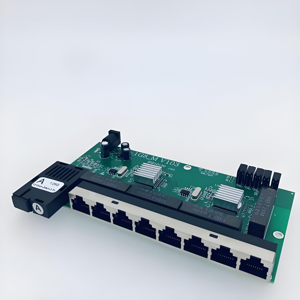
- PCB de enrutador y conmutador
- Módulos de comunicación y dispositivos IoT.
- bluetooth / Placas portamódulos Wi-Fi
Controles industriales
- Controladores lógicos programables PLC
- Módulos de administración de energía
- Placas de circuitos de instrumentación
- Tableros de control de accionamiento de motor
Electrónica automotriz (No críticos para la seguridad)
- Sistemas de infoentretenimiento en el vehículo
- Módulos de control de carrocería
- Tarjetas de interfaz de sensores
Garantía de calidad y cumplimiento de estándares
Normas aplicables
El producto PCB antioxidante OSP de UGPCB sigue estrictamente estos estándares internacionales:
| Estándar | Título | Alcance |
|---|---|---|
| IPC-4555 | Especificación de rendimiento para conservantes orgánicos de soldabilidad a alta temperatura (OSP) para tableros impresos | Requisitos y pruebas del proceso OSP |
| IPC-6012E | Especificación de calificación y rendimiento para tableros impresos rígidos | Calidad y rendimiento del tablero terminado |
| IPC-4101/21 | Especificación para laminado epoxi reforzado con vidrio | Requisitos técnicos del sustrato FR-4 |
| IPC-TM-650 | Manual de métodos de prueba | Varios métodos de prueba de rendimiento. |
| UL 94 V-0 | Inflamabilidad de materiales plásticos | Seguridad retardante de llama del sustrato |
| RoHS 2.0 | Restricción de sustancias peligrosas | Cumplimiento ambiental |
Indicadores clave de calidad
Según los requisitos de IPC, Las métricas de calidad clave incluyen:
- Espesor de la película OSP: 0.2–0,5 µm, tolerancia de uniformidad ≤ ±0.1μm
- Adhesión: ≥4B (IPC-TM-650 2.4.29 prueba transversal)
- Relación de dispersión de soldadura: ≥80% (IPC-TM-650 2.4.1)
- Período de protección contra la oxidación: ≥6 meses (condiciones ambientales)
- Calificación de inflamabilidad: UL 94 V-0
¿Por qué elegir UGPCB para PCB antioxidantes OSP??
Capacidades de fabricación de precisión
- 0.15mm ancho mínimo de traza / 0.20mm de separación mínima
- 0.45mm tamaño mínimo del orificio terminado
- 1.6mm de espesor de tablero estándar con excelente compatibilidad
Control de procesos OSP confiable
- Cumplimiento estricto de IPC-4555 en cuanto a espesor y calidad de la película
- Trazabilidad total durante todo el proceso de fabricación
- Pruebas de soldabilidad y muestreo del espesor de la película para cada lote
Entrega rápida
- Plazo de entrega estándar: 7–10 días laborables
- Admite tanto el muestreo de prototipos como la producción en volumen
Soporte técnico integral
- Revisión de diseño DFM gratuita
- Equipo de ingeniería profesional para orientación en la selección de productos.
Obtenga una cotización hoy
UGPCB ofrece soluciones de placas de circuito PCB antioxidantes OSP de alto valor. Si necesitasmuestreo de prototipos oproducción en volumen, Brindamos soporte técnico profesional y precios competitivos..
📞 Cómo obtener una cotización:
- Envíe sus archivos Gerber y su lista de BOM
- Nuestro equipo de ingeniería responde con una solución personalizada y una cotización dentro de24 horas
- Comprobación DFM gratuita para garantizar que su diseño pase a la primera
Declaración de fuente de datos: Los datos técnicos y los requisitos estándar citados en este documento se derivan principalmente de IPC. (Asociación que conecta industrias electrónicas) estándares que incluyen IPC-4555 “Especificación de rendimiento para conservantes orgánicos de soldabilidad a alta temperatura (OSP) para tableros impresos,” IPC-6012E “Especificación de calificación y rendimiento para tableros impresos rígidos,” IPC-4101/21 “Especificación para laminado epoxi reforzado con vidrio,” IPC-TM-650 “Manual de métodos de prueba,” y UL 94 “Norma para pruebas de inflamabilidad de materiales plásticos para piezas de dispositivos y electrodomésticos.” Algunos parámetros de proceso hacen referencia a datos técnicos disponibles públicamente de los principales fabricantes de PCB.. Todos los datos han sido verificados para su precisión..













