

1. Descripción general del producto: ¿Qué es una PCB de aspiradora inalámbrica??
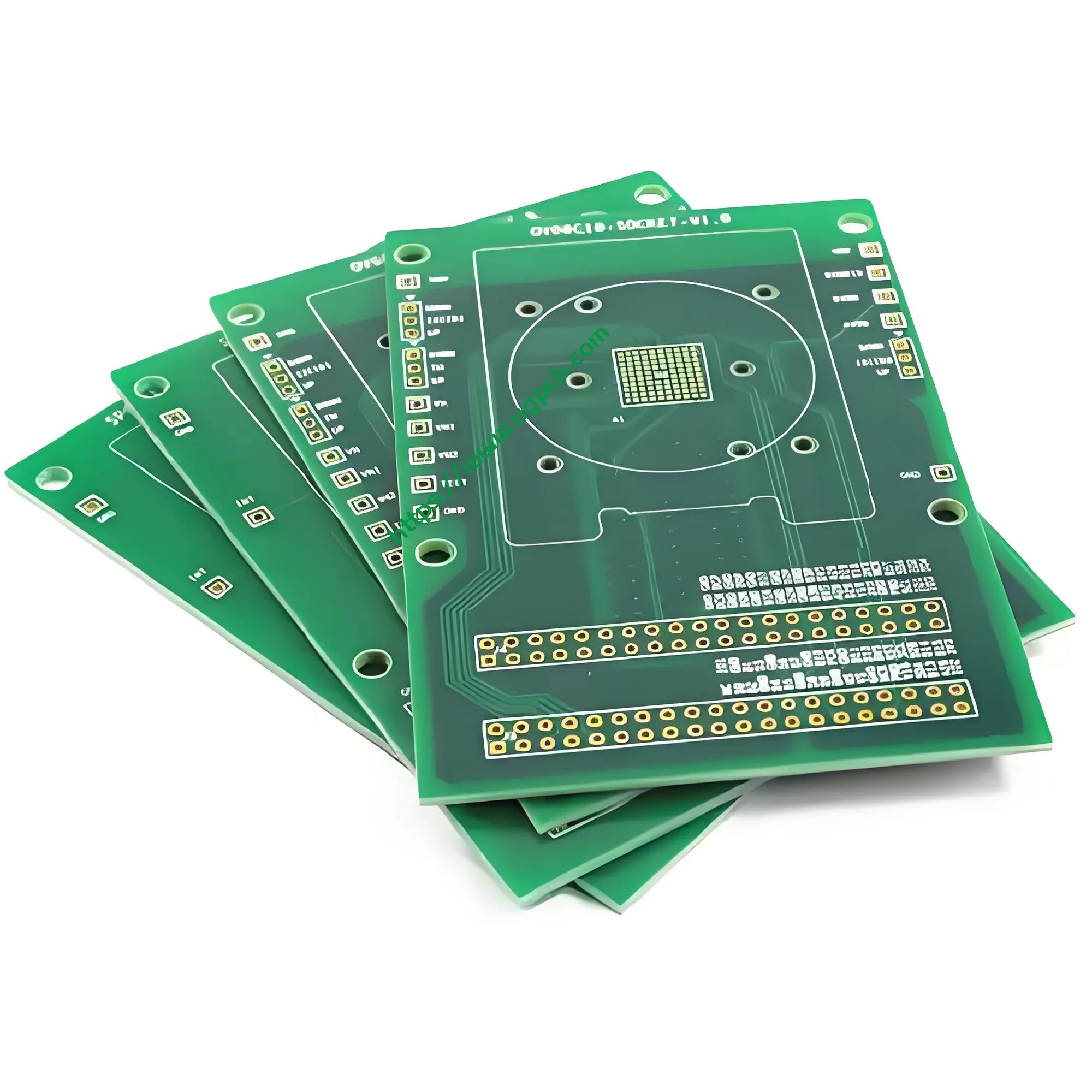
Una PCB de aspiradora inalámbrica (Placa de circuito impreso) Es el componente electrónico central responsable del control del accionamiento del motor., gestión de energía, interacción del usuario, y protección de seguridad dentro de una aspiradora inalámbrica. En términos simples, Sirve como “cerebro” y “centro nervioso” del dispositivo.. Recibe comandos de botones., controla la velocidad del motor sin escobillas, gestiona la carga y descarga de la batería, monitorea el estado de funcionamiento, e implementa múltiples protecciones de seguridad.
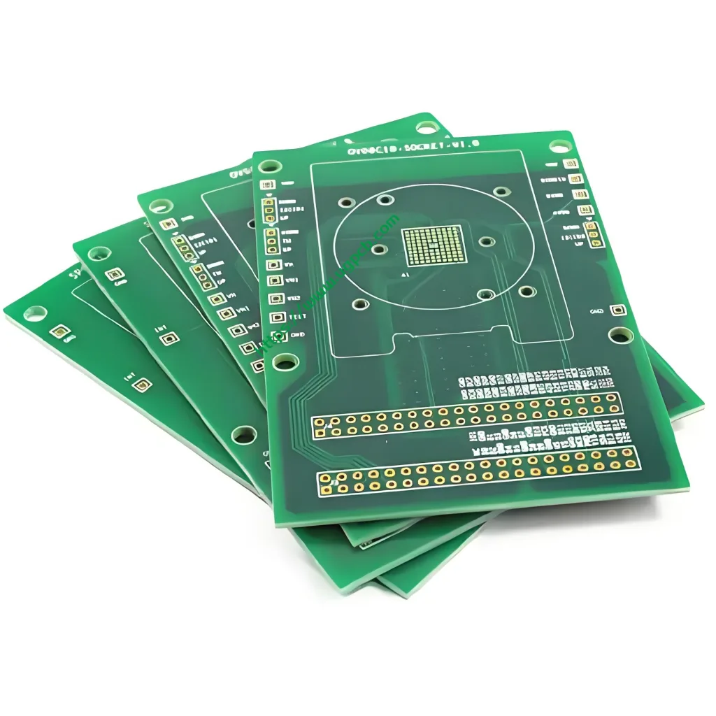
UGPCB presenta esta PCB para aspiradora inalámbrica: una 2-placa de circuito impreso rígida de capa Diseñado específicamente para equipos de limpieza portátiles.. se utiliza Laminado revestido de cobre epoxi de vidrio FR-4 como material base. El espesor del tablero es de 1,0 mm., y las dimensiones son 86.37 × 72,6 mm. Este tamaño compacto encaja perfectamente en los espacios internos reducidos de las aspiradoras inalámbricas de mano y tipo varilla..
Según IPC-6012F Especificación de calificación y rendimiento para tableros impresos rígidos, este producto cae bajo el cartón rígido impreso a doble cara (con agujeros pasantes chapados) categoría. Como parte clave de la ventanilla única de UGPCB tarjeta de circuito impreso soluciones, Este producto cumple con los estándares internacionales IPC desde el diseño hasta la fabricación y el control de calidad.. Proporciona a los fabricantes de aspiradoras una alta confiabilidad, rentable tarjeta de circuito impreso solución.
2. Clasificación de productos: Posicionamiento científico y categorización de la industria
Según IPC-6012F y PCB estándar sistemas de clasificación de la industria, Este producto se puede clasificar científicamente de la siguiente manera.:
| Dimensión de clasificación | Categoría |
|---|---|
| Por estructura | Cartón rígido impreso a doble cara (con agujeros pasantes chapados) |
| Por material base | Laminado revestido de cobre de vidrio tejido epoxi FR-4 (Cumple con IPC-4101) |
| Por recuento de capas | 2-tablero de capas (PCB de doble cara) |
| Por acabado superficial | HASL sin plomo (Nivelación de soldadura por aire caliente) |
| Por clasificación de inflamabilidad | UL 94 V-0 |
| Por aplicación | Electrónica de consumo / tablero de control de pequeños electrodomésticos (aspiradora PCBA) |
Dentro de la industria electrónica de aspiradoras, este producto pertenece alPCBA de control y accionamiento del motor categoría. Junto con el tablero de control principal y el tablero de administración de energía., Forma los tres módulos de circuito central de una aspiradora inalámbrica..
3. Parámetros técnicos clave
3.1 Material base y espesor del tablero
- Materia prima: FR-4 (laminado revestido de cobre epoxi reforzado con fibra de vidrio)
- Grosor del tablero: 1.0milímetros
FR-4 es el sustrato rígido más utilizado en la industria de PCB. Para IPC-4101, FR-4 ofrece un excelente aislamiento eléctrico, resistencia mecánica, y resistencia al calor. El FR-4 estándar tiene una temperatura de transición vítrea (tg) de 130–140°C. Para IPC-6012, el rango de tolerancia para tableros de 1,0 mm de espesor es ±0,1 mm.
3.2 Número de capas y dimensiones
- Recuento de capas: 2 capas (tablero de doble cara)
- Dimensiones: 86.37 × 72.6 milímetros
La estructura de 2 capas controla eficazmente los costos de fabricación y al mismo tiempo ofrece un rendimiento eléctrico sólido.. Esto lo convierte en la opción principal para los paneles de control inalámbricos de aspiradoras.. El compacto 86.37 × Las dimensiones de 72,6 mm están optimizadas para el espacio limitado dentro de las aspiradoras..
3.3 Ancho/espaciado del trazado y tamaño mínimo del orificio
- Tamaño mínimo de agujeros: 0.45milímetros
- Ancho/Espaciado del trazo: 0.45milímetros / 0.391milímetros
Según IPC-2221CNorma genérica sobre diseño de tableros impresos, El diseño de ancho de pista y espaciado debe considerar el rendimiento eléctrico., capacidad de carga de corriente, y capacidad de fabricación. El tamaño mínimo del orificio de 0,45 mm admite una soldadura confiable de componentes DIP convencionales y piezas de orificio pasante..
Para capacidad de carga de corriente, la fórmula estándar de la industriaI = k·ΔT^0,44·A^0,725 (donde A es el área de la sección transversal de la traza) muestra que con 1oz de cobre, un 0,45 mm (aprox. 18mil) la traza puede transportar entre 1,8 y 2,0 A. La PCB de la aspiradora inalámbrica utiliza este ancho de traza para señales de accionamiento del motor y señales de control., asegurando un funcionamiento estable a largo plazo.
3.4 Espesor de lámina de cobre
- Espesor de lámina de cobre: 1/1 ONZ (1 onzas en ambas capas exteriores)
1oz de lámina de cobre (aprox. 35μm) es la configuración estándar para PCB de electrónica de consumo. Logra un excelente equilibrio entre la capacidad de transporte de corriente, conductividad térmica, y costo.
3.5 Acabado superficial
- Acabado superficial: HASL sin plomo (Nivelación de soldadura por aire caliente)
HASL es un acabado de superficie de PCB maduro y económico. HASL sin plomo cumple con los requisitos medioambientales RoHS. Según los estándares IPC, HASL sin plomo suele tener un espesor de capa de estaño de 1 a 40 μm, con procesos convencionales controlados a 5–25μm. Este acabado ofrece una excelente soldabilidad. (humectabilidad) y una buena vida útil de hasta 12 meses.
3.6 Máscara de soldadura y leyenda
- Color de máscara de soldadura: tinta verde
- Color de leyenda: Blanco
La máscara de soldadura verde es la opción más popular de la industria. Proporciona una excelente protección de aislamiento y alto contraste para AOI (Inspección óptica automatizada). Las leyendas blancas son claras y fáciles de leer., Facilitar la colocación de componentes y el mantenimiento futuro..
4. Pautas de diseño: Siguiendo los estándares IPC-2221C
Una PCB de aspiradora inalámbrica bien diseñada debe seguir estos principios básicos (según IPC-2221C):
4.1 Diseño de rendimiento eléctrico
- Ancho de seguimiento de energía: Calcular usando la fórmula I = k·ΔT^0,44·A^0,725 para garantizar que el aumento de temperatura se mantenga por debajo de 10 °C con la corriente operativa máxima.
- Integridad de señal: Utilice un ancho de traza de 0,45 mm para las señales de control para garantizar la transmisión completa de las señales de control de velocidad PWM y las señales del sensor..
- Diseño de puesta a tierra: Utilice estrategias de puesta a tierra de un solo punto o de puesta a tierra dividida para evitar interferencias del bucle de alimentación con el bucle de control..
4.2 Diseño de gestión térmica
Las aspiradoras inalámbricas generan una cantidad significativa de calor a partir de los MOSFET durante el funcionamiento. El diseño de PCB debe abordar esto mediante:
- Colocación de matrices térmicas debajo de dispositivos de energía..
- Ampliar las trazas de alta corriente o agregar cobre expuesto para una mejor disipación del calor.
- Uso de tablero de 1,0 mm de espesor para equilibrar la conductividad térmica y la resistencia mecánica.
4.3 Diseño de estructura mecánica
El 86.37 × Las dimensiones de 72,6 mm deben coincidir exactamente con la carcasa de la aspiradora.. Las posiciones de los orificios de montaje y las ubicaciones de los conectores deben cumplir con los requisitos de diseño estructural.. El tamaño mínimo del orificio de 0,45 mm admite soldadura a través de orificios para varios componentes y conectores DIP..
5. Principio de trabajo
La PCB de la aspiradora inalámbrica funciona a través de los siguientes procesos centrales:
① Entrada y gestión de energía: La batería de litio (normalmente 21,6 V o 25,2 V) pasa a través del circuito de administración de energía en la PCB. Esto proporciona voltajes estables al chip de control principal y a los circuitos del controlador..
② Cálculo del chip de control principal: La MCU (microcontrolador) en la PCB recibe comandos de botón. Calcula y emite señales de accionamiento trifásico utilizando FOC (Control orientado al campo) o algoritmos de control de onda cuadrada.
③ Impulsión del motor: Las señales del variador son amplificadas por dispositivos de potencia MOSFET.. Estas señales luego impulsan el motor de CC sin escobillas. (BLDC) girar a alta velocidad, generando el flujo de aire necesario para la succión.
④ Comentarios y protección: La PCB monitorea continuamente la corriente del motor., voltaje de la batería, temperatura, y otros parámetros. Cuando detecta condiciones anormales como sobrecorriente, sobre temperatura, subtensión, o bloqueo del rotor, ejecuta inmediatamente acciones de protección.
6. Materiales utilizados
| Componente | Material | Descripción |
|---|---|---|
| sustrato | Epoxi de vidrio FR-4 | Cumple con IPC-4101 |
| Capa conductora | Lámina de cobre electrolítico (1onz) | 1oz en ambas capas exteriores |
| Máscara de soldadura | Tinta fotoimagen verde | Protección de aislamiento, resistencia a la oxidación |
| Acabado superficial | Aleación HASL sin plomo | Cumplimiento de ROHS |
| Tinta de leyenda | Tinta epoxi blanca | Alto contraste, resistente al calor |
El sustrato FR-4 lleva una certificación UL 94 V-0 calificación de inflamabilidad. En la prueba de quemado vertical, la llama se apaga dentro 10 segundos después de la eliminación, sin goteos ardientes. Esta característica es crítica para alta potencia., Dispositivos que funcionan con baterías como aspiradoras inalámbricas.. Reduce significativamente el riesgo de incendio causado por fallas en el circuito..
7. Especificaciones de rendimiento
7.1 Rendimiento eléctrico
| Parámetro | Especificación | Estándar de referencia |
|---|---|---|
| Resistencia de aislamiento | ≥10^6 MΩ | IPC-6012F |
| Tensión soportada dieléctrica | Hasta 500V (dependiente del diseño) | IPC-2221C |
| Resistencia a la conducción | ≤50mΩ (típico) | IPC-6012F |
| Impedancia característica | Controlable bajo pedido (50Ω/90Ω/100Ω) | IPC-2221C |
7.2 Rendimiento térmico
| Parámetro | Especificación | Estándar de referencia |
|---|---|---|
| Temperatura de transición vítrea (tg) | ≥135°C (método DSC) | IPC-TM-650 2.4.25 |
| Resistencia al calor de soldadura | 288°C / 10s, Sin delaminación | IPC-4101 |
| CTE del eje z (CTEz) | ≤65 ppm/°C (50–260°C) | IPC-4101 |
7.3 Rendimiento mecánico
| Parámetro | Especificación | Estándar de referencia |
|---|---|---|
| Tolerancia del espesor del tablero | ±0,1 mm | IPC-6012 |
| Tolerancia del tamaño del agujero | ±0,05 mm | IPC-6012F |
| Calificación de inflamabilidad | UL 94 V-0 | UL 94 |
7.4 Fiabilidad
- Prueba de soldabilidad: Cumple con IPC-J-STD-003
- Prueba de envejecimiento: 500 horas en condiciones de doble 85 (85°C / 85%RH) sin anormalidades
8. Características estructurales
8.1 2-Ventajas del tablero de capas
La capa superior lleva los componentes principales y los rastros de señal.. La capa inferior maneja componentes auxiliares y vertidos de cobre a tierra/potencia.. El diseño de 2 capas logra elmejor costo ymáxima confiabilidad Balanza para funciones de control inalámbrico de aspiradora..
8.2 Orificio pasante chapado (PTH) Proceso
Todos los orificios pasantes utilizan el proceso de orificio pasante enchapado.. Esto garantiza una interconexión fiable entre las capas superior e inferior.. También proporciona soporte mecánico sólido y conexión eléctrica para componentes DIP..
8.3 Proceso de puente de máscara de soldadura
La máscara de soldadura verde forma puentes entre las almohadillas adyacentes. Esto evita cortocircuitos de soldadura y mejora el rendimiento de colocación SMT..
9. Flujo del proceso de fabricación
UGPCB sigue estrictamente los estándares IPC-6012F para controlar cada paso de producción.:
① Inspección de material entrante →② Creación de circuito de capa interna (para tableros de 2 capas, esta es directamente la capa exterior) →③ Laminación (no aplicable para tableros de 2 capas) →④ Perforación (tamaño mínimo del agujero 0,45 mm) →⑤ Deposición de cobre no electrolítica / Revestimiento de paneles →⑥ Circuito de capa exterior →⑦ Patrón de revestimiento →⑧ Grabado →⑨ Máscara de soldadura (tinta verde) →⑩ Acabado superficial (HASL sin plomo) →⑪ Leyenda (personajes blancos) →⑫ Enrutamiento de perfil (86.37 × 72,6 mm) →⑬ Prueba eléctrica →⑭ Inspección final (para IPC-A-600) →⑮ Embalaje y envío
Cada lote se sometePrueba de sonda voladora opruebas de accesorios dedicados para asegurar 100% sin circuitos abiertos o cortocircuitos.
10. Escenarios de aplicación
10.1 Aplicaciones primarias
- Aspiradoras inalámbricas de mano: Accionamiento y control de motores en espacios compactos
- Aspiradoras inalámbricas estilo varilla: Gestión de batería y accionamiento de motor sin escobillas.
- aspiradoras robotizadas: Control de navegación y accionamiento motorizado.
- aspiradoras de autos: 12Adaptación y control de potencia V/24V
- Dispositivos de limpieza inteligentes: Conectividad IoT y control inteligente
10.2 Ejemplos de productos finales
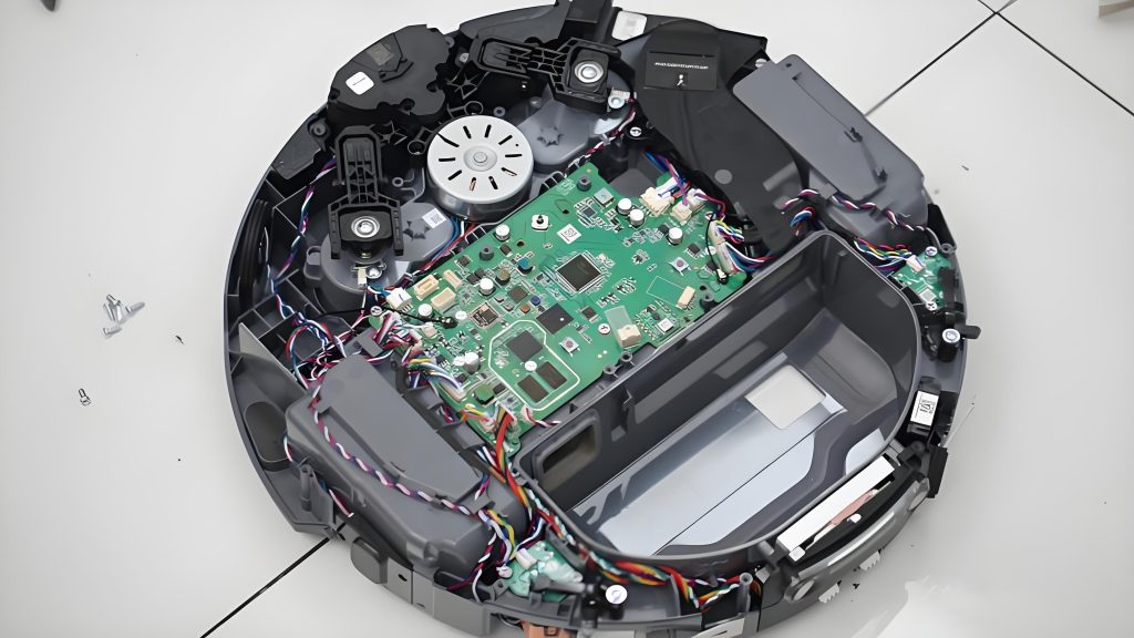
Este PCB puede usarse ampliamente en tableros de control y tableros de controladores para aspiradoras inalámbricas y dispositivos de limpieza similares de marcas como Xiaomi., Dyson, Tineco, y leifheit.
11. Por qué elegir la PCB para aspiradora inalámbrica de UGPCB?
✅Cumplimiento de estándares internacionales: Diseño, fabricación, e inspección cumplen totalmente con IPC-6012F, IPC-A-600, IPC-2221C, y otras normas internacionales
✅UL 94V-0 Seguridad contra incendios: El sustrato FR-4 logra el índice de combustión vertical más alto, garantizar la seguridad del dispositivo

✅Proceso ecológico sin plomo: El acabado superficial HASL sin plomo cumple con las directivas medioambientales RoHS y REACH.
✅Capacidad de fabricación comprobada: UGPCB ofrece servicios integrales desde el diseño y la fabricación de PCB hasta el ensamblaje de PCBA.
✅Estricto control de calidad: Inspección visual según IPC-A-600 y 100% Las pruebas eléctricas garantizan la calidad del envío.
✅Dimensiones compactas optimizadas: El 86.37 × El tamaño de 72,6 mm se adapta perfectamente al espacio interno de varias aspiradoras inalámbricas
12. Obtenga una cotización y muestras hoy
UGPCB se compromete a proporcionar alta precisión, Soluciones de PCB y PCBA de alta confiabilidad para fabricantes de productos electrónicos en todo el mundo. Si necesitas PCB desnudos, PCBA completamente ensamblada, o Servicios integrales desde el diseño hasta la producción en masa., UGPCB tiene la experiencia para apoyarlo.
📧Póngase en contacto con UGPCB para obtener una cotización personalizada hoy →
- Sitio web: www.ugpcb.com
- Modificaciones y optimizaciones de diseño personalizadas disponibles
- DFM gratis (Diseño para la fabricación) revisar
- Prototipos rápidos y producción en volumen disponibles
Declaración de fuente de datos
Los estándares técnicos y los datos citados en este artículo provienen de las siguientes organizaciones autorizadas.:
- PCI (Asociación que conecta industrias electrónicas): IPC-6012F Especificación de calificación y rendimiento para tableros impresos rígidos, IPC-A-600 Aceptabilidad de los tableros impresos, IPC-2221C Norma genérica sobre diseño de tableros impresos, IPC-4101 Especificación de Materiales Base para Tableros Impresos Rígidos y Multicapa, IPC-TM-650 Manual de métodos de prueba
- UL (Laboratorios aseguradores): UL 94 Norma de seguridad de inflamabilidad de materiales plásticos para piezas de dispositivos y electrodomésticos –V-0 clasificación
- Fórmula de ingeniería estándar de la industria: Fórmula de capacidad de carga de corriente de PCB I = k·ΔT^0,44·A^0,725













