

In the era of data-intensive and ultra-high-speed signal transmission, a Printed Circuit Board (tarjeta de circuito impreso) is far more than a simple component carrier; it is the critical architecture defining system performance limits. For demanding applications like high-speed networking, artificial intelligence computing, and advanced test instrumentation, standard FR-4 materials fall short. UGPCB addresses this need with our advanced 22-layer multilayer PCB built on Panasonic Megtron-6 R-5775G laminate, engineered to meet challenges of high frequency, low loss, and complex interconnectivity.
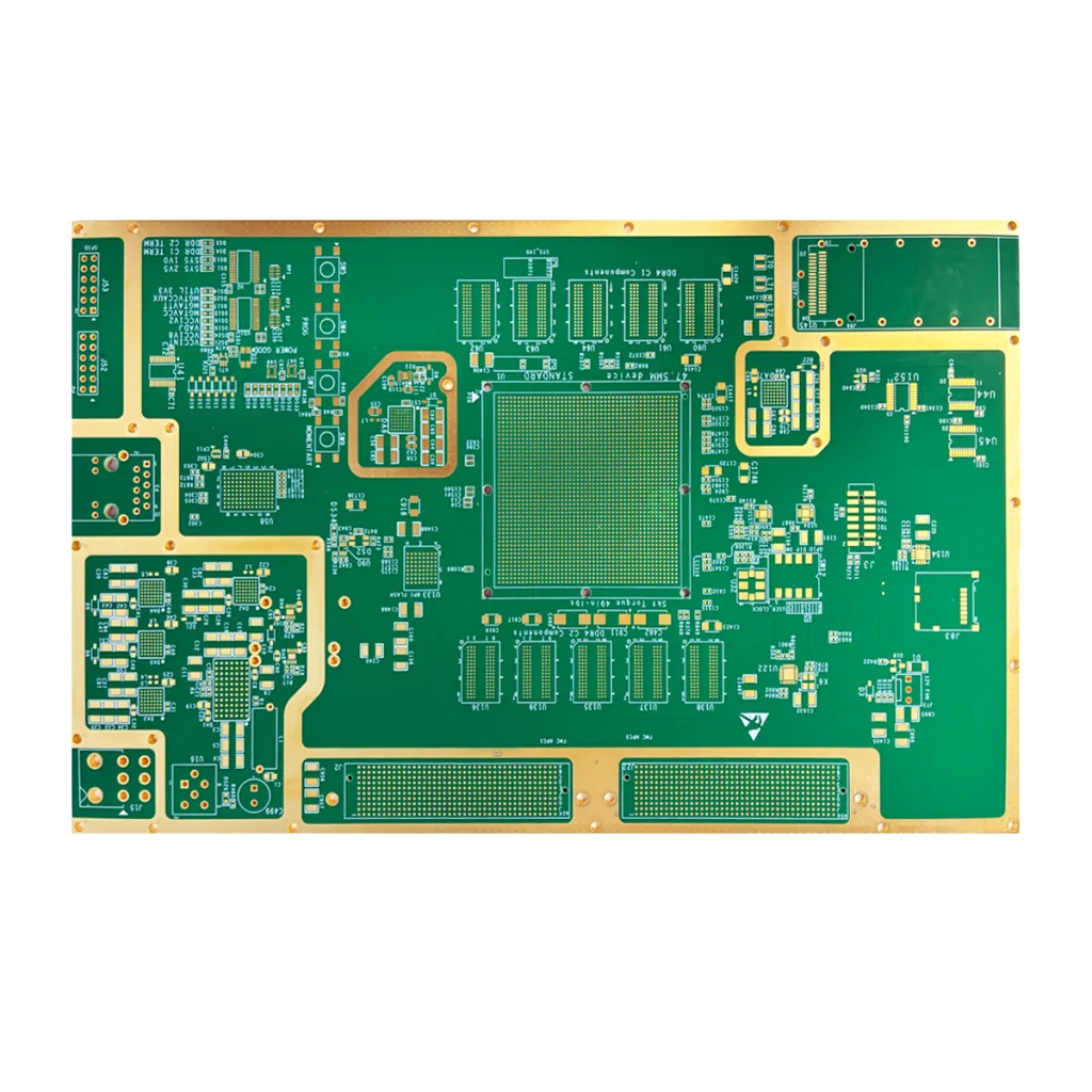
1.UGPCB’s 22-Layer Megtron-6 High-Speed PCB Descripción general del producto & Definición
Este producto es un 22-layer High-Density Interconnect (IDH) placa de circuito impreso rígida. Its core advantage lies in the use of a premium-grade, de alta velocidad, low-loss laminate—Panasonic’s Megtron-6 R-5775G. Combined with a robust 2.0mm board thickness and precision lamination technology, it creates a high-end interconnection platform capable of handling high-frequency signals above 10GHz with exceptional signal integrity and power integrity.

2. Consideraciones críticas de diseño
Designing such an advanced placa de circuito multicapa requires focus on:
-
Control de impedancia: Precise calculation and control of single-ended and differential impedance to ensure consistent signal propagation within the Megtron-6 dielectric.
-
Optimización de apilamiento: The intelligent arrangement of the 22 conductive layers (22capas)—including signal, fuerza, and ground planes—is crucial for maximizing shielding and minimizing crosstalk in this high-layer count PCB.
-
Gestión Térmica: The 2.0mm board thickness and multilayer structure aid heat distribution. Sin embargo, strategic use of thermal vias remains essential for high-power IC areas.
-
High-Frequency Routing: Employing microstrip or stripline configurations, avoiding acute angle turns, and leveraging the low-profile copper foil of Megtron-6 to reduce losses from skin effect.
3. Cómo funciona & Estructura
A PCB’s primary function is to provide electrical connectivity and signal transmission between components via etched copper traces on an insulating substrate. Este 22-placa PCB de capa structure resembles a precise “multi-layer sandwich”:
-
Capas internas: Use H/HOZ (aproximadamente 1/1 oz or 35µm) copper for core power, planos de tierra, and some internal signal routing.
-
Capas exteriores: Use 1/1 oz copper for mounting primary components and routing critical signal traces.
-
Dielectric Layers: All insulating prepreg materials are Panasonic Megtron-6 R-5775G, whose low Dielectric Constant (Dk) y factor de disipación (df) ensure superior high-speed signal transmission.
-
Acabado superficial: Oro de inmersión de níquel químico (ACEPTAR) en 2 micro-inches (2tu”). This provides a flat, solderable surface, excellent oxidation resistance, and good wire-bonding capability, ideal for high-density BGA packages and RF connectors.
4. Material central: Panasonic Megtron-6 R-5775G
This is the heart of this advanced PCB material. Megtron-6 is Panasonic’s next-generation, de alta velocidad, low-loss circuit board material series.
-
Rendimiento clave: Features an extremely low Dielectric Constant (Dk~3.5) and ultra-low Dissipation Factor (Df~0.0015 @ 10GHz), significantly outperforming standard FR-4. Its high Glass Transition Temperature (tg) ensures superior thermal stability and dimensional consistency during high-temperature reflow soldering processes.
-
Application Fit: Optimized for high-speed digital signals (10Gbps+ to 56/112Gbps) and millimeter-wave RF applications.
| Item | Test method | Condición | Unidad | MEGTRON6 R-5775(norte) Low Dk glass cloth |
MEGTRON6 R-5775 Normal glass cloth |
|
| Glass transition temp.(tg) | DSC | A | °C | 185 | 185 | |
| Thermal decomposition temp.(td) | TGA | A | °C | 410 | 410 | |
| CTE x-axis | α1 | IPC-TM-650 2.4.24 | A | ppm/°C | 14-16 | 14-16 |
| CTE y-axis | 14-16 | 14-16 | ||||
| CTE z-axis | α1 | IPC-TM-650 2.4.24 | A | 45 | 45 | |
| α2 | 260 | 260 | ||||
| T288(with copper) | IPC-TM-650 2.4.24.1 | A | mín. | >120 | >120 | |
| Constante dieléctrica(Dk) | 12GHz | Balanced-type circular disk resonator |
C-24/23/50 | - | 3.4 | 3.6 |
| factor de disipación(df) | 0.004 | 0.004 | ||||
| Water absorption | IPC-TM-650 2.6.2.1 | D-24/23 | % | 0.14 | 0.14 | |
| Flexural modulus | Fill | JIS C 6481 | A | GPA | 18 | 19 |
| Fuerza de pelado* | 1onz(35μm) | IPC-TM-650 2.4.8 | A | kN/m | 0.8 | 0.8 |
5. Características clave & Actuación
-
Ultra-Low Signal Loss: Megtron-6 material ensures maximum efficiency in high-frequency signal transmission with minimal attenuation.
-
Excellent Thermal & Dimensional Stability: High Tg value combined with a 2.0mm thick board suits high-temperature, high-power application environments.
-
High-Density Interconnect Capability: The 22-layer design provides abundant routing channels, supporting complex interconnections for large-scale chips (p.ej., FPGAs, GPU).
-
Precise Impedance & Layer-to-Layer Registration: Mature manufacturing processes guarantee consistent electrical performance across the PCB multicapa.
-
Soldabilidad superior & Vinculación: The 2u” ENIG finish ensures highly reliable solder joints and is suitable for precision SMT assembly.
6. Scientific Classification & Aplicaciones primarias
-
Scientific Classification:
-
Por recuento de capas: High Multilayer PCB (Típicamente >10 capas).
-
Por material: PCB de alta velocidad / PCB de alta frecuencia / PCB de baja pérdida.
-
Por tecnología: PCB HDI (Subject to specific design features like blind/buried vias).
-
Por rigidez: PCB rígido.
-
-
Aplicaciones primarias & Casos de uso:
-
High-Speed Networking Equipment: Core backplanes and motherboards for 400G/800G optical modules, enrutadores de alta gama, y cambia.
-
Computación avanzada & Almacenamiento: AI server boards, Informática de alto rendimiento (HPC) clusters, enterprise SSD controller boards.
-
Aeroespacial & Sistemas de radar: RF front-ends and signal processing units for avionics communication and phased array radar systems.
-
Advanced Test & Instrumentos de medición: Mainboards within high-speed oscilloscopes, analizadores de espectro, y generadores de señal.
-
7. Production Flow Overview
UGPCB se adhiere a un estricto Proceso de fabricación de PCB to ensure quality:
Material Cutting → Inner Layer Imaging → Lamination (22-Alineación de capas & Vinculación) → Drilling → Hole Metallization → Outer Layer Imaging → Pattern Plating → Etching → Solder Mask Application → ENIG Surface Finish → Routing / Scoring → Electrical Testing → Final Inspection (AOL)
Every step is supported by high-precision equipment, with multiple quality control checkpoints integrated into the proceso de fabricación de PCB, ensuring this 22-layer Megtron-6 PCB meets the highest standards from design to delivery.
Don’t let base materials limit your innovative designs.
Whether you’re developing next-gen communication hardware or tackling frontier computing challenges, UGPCB 22-layer high-performance PCB solution is your reliable hardware foundation. We provide not just a product, but full-spectrum support from PCB design consultation to rapid prototyping and volume production.
Click to request a quote and receive expert technical documentation. Power your project with a superior core!


