
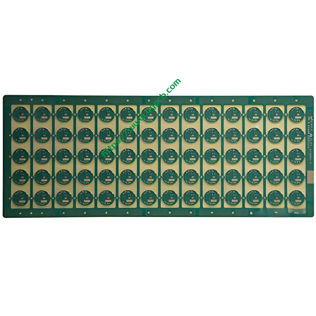
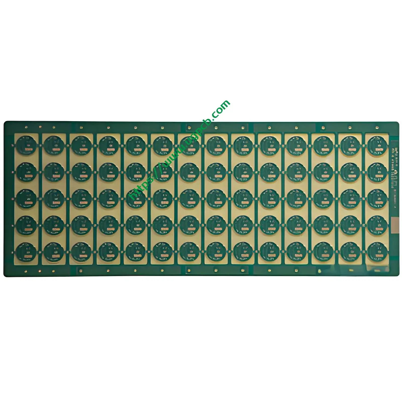
Introduction to UGPCB Micro PCB Solutions
UGPCB specializes in manufacturing Micro PCB y Ultra Small Size PCB productos, designed for high-density, compact electronic applications. Estos PCB feature a 0.6mm finished thickness, 4-layer construction, and precise 6mil trace/space capabilities, making them ideal for advanced PCB and tarjeta de circuito impreso projects in industries like IoT, dispositivos medicos, y electrónica de consumo. With gold-plated surfaces and FR-4 material, UGPCB ensures reliability and performance for demanding environments.
What Are Micro PCBs and Ultra Small Size PCBs?
Micro PCBs y Ultra Small Size PCBs refer to placas de circuito impreso with exceptionally small dimensions, such as UGPCB’s minimum finished board size of 0.5mm x 1.0mm. These boards support high component density and are engineered for applications where space is limited. They are a key component in miniaturized diseño de PCB y advanced Asamblea de PCBA, enabling sleeker and more efficient electronic products.
Key Design Considerations for Micro PCBs
When designing Micro PCBs, engineers must account for several factors to ensure functionality and manufacturability:
-
Trace and Space Requirements: UGPCB’s minimum trace and space of 6mil (0.15milímetros) demand precise diseño de PCB técnicas to avoid signal interference.
-
Layer Management: The 4-layer structure allows for separated power, suelo, and signal layers, optimizing PCB de alta velocidad actuación.
-
Tratamiento superficial: Gold-plating with 0.2μm thickness enhances conductivity and corrosion resistance, critical for reliable PCBA processes.
-
Selección de material: FR-4 material provides excellent thermal and mechanical stability, secundario durable fabricación de PCB.
How Micro PCBs Work: Basic Principles
Micro PCBs function by interconnecting electronic components through conductive copper traces embedded in insulating layers. In UGPCB’s 4-layer design, signals are routed efficiently to minimize noise and crosstalk, secundario complex PCB circuitry in ultra-small formats. This makes them suitable for low-power PCB applications y high-density PCBA integration, where precise electrical pathways are essential.
Applications and Uses of Micro PCBs
UGPCB’s Micro PCBs are versatile and used across various sectors:
-
Tecnología portátil: For fitness trackers and smartwatches requiring compact PCB solutions.
-
Internet de las cosas (IoT): Enabling small sensors and connected devices with efficient PCBA designs.
-
Electrónica médica: In implantable devices and diagnostic tools where reliable micro PCB performance es crítico.
-
Electrónica de Consumo: Powering smartphones, drones, and other portable gadgets with space-saving PCB layouts.
Classification of Micro PCBs
Micro PCBs can be categorized based on their specifications:
-
By Size: Ultra small size PCBs (p.ej., sub-1mm dimensions) versus standard micro PCBs.
-
Por recuento de capas: De una sola cara, de dos caras, o multicapa (like UGPCB’s 4-layer boards) para custom PCB projects.
-
Por aplicación: High-frequency, flex-rigid, or standard FR-4 boards tailored for specialized PCBA services.
Materials Used in UGPCB Micro PCBs
UGPCB employs Material FR-4 for its Micro PCBs, a flame-retardant epoxy laminate known for:
-
High Dielectric Strength: Ideal for insulated PCB designs.
-
Resistencia térmica: Withstands soldering temperatures during Asamblea de PCBA.
-
Rentabilidad: Balances performance and affordability for volume PCB production.
Performance Specifications of UGPCB Micro PCBs
Key performance metrics include:
-
Espesor terminado: 0.6milímetros, secundario slim PCB profiles for tight spaces.
-
Espesor de cobre: 1ONZ, ensuring adequate current carrying capacity for stable PCB operations.
-
Durabilidad: Gold-plating (0.2μm) resists oxidation, enhancing long-term PCBA reliability.
-
Operational Range: Adecuado para wide-temperature PCB applications, from -50°C to 110°C.
Structural Details of 4-Layer Micro PCBs
UGPCB’s 4-layer Micro PCBs consist of:
-
Top and Bottom Layers: For component placement and routing.
-
Capas internas: Dedicated to power and ground planes, reducing EMI in noise-sensitive PCB systems.
-
Via Structures: Microvias or through-holes facilitate inter-layer connections, crucial para complex PCBA layouts.
Key Features and Benefits of UGPCB Micro PCBs
-
Ultra-Small Size: Habilita miniaturized electronics with boards as small as 0.5mm x 1.0mm.
-
Alta precisión: 6mil trace/space supports detailed PCB artwork y fine-pitch PCBA components.
-
Confiabilidad mejorada: Gold-plating and FR-4 material ensure robust PCB performance in harsh conditions.
-
Cost-Efficiency: Streamlined production processes reduce costs for high-volume PCB orders.
Production Process of Micro PCBs

UGPCB’s manufacturing workflow includes:
-
Design and Fabrication: Using CAD software for PCB layout optimization.
-
Layer Lamination: Bonding FR-4 layers with copper foils.
-
Grabado y perforación: Creating traces and vias with 6mil precision.
-
Tratamiento superficial: Applying gold-plating for corrosion-resistant PCB finishes.
-
Prueba y control de calidad: Ensuring each board meets industry PCB standards para error-free PCBA integration.
Common Use Scenarios for Micro PCBs
These PCBs are ideal for:

-
Portable Devices: Such as headphones and GPS units, dónde lightweight PCB designs are essential.
-
Industrial Sensors: For monitoring systems requiring alta densidad PCB components.
-
Electrónica automotriz: In control modules leveraging durable PCBA assemblies.
-
Aerospace Systems: Dónde reliable micro PCB performance under extreme conditions is mandatory.


