
나. 시장 촉매제: NVIDIA의 M10 테스트를 통해 초고속 시대의 PCB 출시
3월 2026, AI 리더인 NVIDIA의 공급망 움직임이 전자 산업에 파급력을 일으켰습니다.. 차세대 Rubin 플랫폼은 M10에 대한 공급업체 테스트를 공식적으로 시작했습니다., 새로운 구리 클래드 라미네이트 (CCL) 재료. 이는 단순한 재료 업그레이드 그 이상입니다.. 그것은 신호를 보낸다 PCB 업계 공식 고주파수 진출, 고속 시대. 이 새로운 시대는 AI에 의해 주도되며 초저손실 및 탁월한 신호 무결성으로 정의됩니다..
M10 테스트는 Rubin Ultra 및 Feynman 플랫폼의 중요한 구성 요소를 대상으로 합니다.. 여기에는 직교 백플레인 및 스위치 블레이드 마더보드가 포함됩니다.. 이전 M9세대에 비해, M10은 여러 공급업체를 소개합니다.. 이는 단일 소스 종속성을 깨뜨립니다.. 더 중요한 것은, 새로운 성능 벤치마크를 설정합니다.. 신호 손실은 감소할 것으로 예상됩니다. 30-40% 기존 FR-4 PCB와 비교. 이는 800G/1.6T 광학 모듈 및 고성능 컴퓨팅의 엄격한 전송 속도 및 열 관리 요구 사항을 충족하는 데 중요합니다.. 테스트가 원활하게 진행된다면, 하반기 양산 예정 2027. 이는 AI 서버 PCB 소재에 대한 대규모 조달의 새로운 주기를 촉발할 것입니다..
II. PCB: 단순한 것 이상 “해골,” 그것은 “신경 센터” AI컴퓨팅의
이 변화를 이해하려면, 먼저 PCB 자체를 살펴봐야 합니다.. PCB는 다음을 의미합니다. 인쇄 회로 기판. 종종 “전자제품의 어머니.” 절연 기판에 전도성 회로와 연결 구멍을 식각하는 캐리어입니다., 동박적층판처럼.
핵심 기능은 물리적 지원 그 이상입니다.:
-
전기 연결: 모든 구성 요소에 안정적인 회로 연결을 제공합니다.. 여기에는 CPU가 포함됩니다., GPU, 메모리, 저항기, 커패시터.
-
신호 전송 및 전력 분배: 왜곡 없이 고속 신호 전송을 보장합니다.. 또한 모든 구성 요소에 전력을 정확하게 분배합니다..
-
열 방출 및 차폐: 고전력 AI 칩 아래, PCB는 효율적인 열 경로 역할을 합니다.. 또한 시스템 안정성을 보장하기 위해 전자기 차폐 기능을 제공합니다..
고성능 PCB가 없는 경우, 스마트폰은 그렇게 얇지 않을 것이다. 자동차 전자 장치는 스마트하지 않습니다.. AI 서버의 엄청난 컴퓨팅 능력은 불가능할 것이다. AI 컴퓨팅 수요가 급증함에 따라, PCB 기술이 진화하고 있다. 전통적인 다층 기판에서 고급 디자인으로 이동하고 있습니다.. 여기에는 더 높은 레이어 수가 포함됩니다., 고밀도 상호 연결 (HDI), 강성-플렉스 구조.
III. 2026 PCB 산업 현황 및 경쟁 환경: 에이 “2계층” 중국 제조업이 지배하는 세계
에 의해 2026, PCB 산업 체인은 명확하게 보여줍니다 “AI 기반” 형질. 이제 글로벌 경쟁 환경은 급격히 분열되었습니다.. 한쪽은 중국, 압도적인 제조 규모. 반대편에는 일본이 있다, 대만, 그리고 한국, 고급 소재 분야를 선도하는.
1. 고도로 최적화된 수요 구조
AI 서버의 폭발적인 성장은 PCB 수요를 직접적으로 재편했습니다.. 데이터에 따르면 AI 서버는’ PCB 수요 비중이 전년 대비 크게 증가 15% ~에 2025 이상으로 25% ~에 2026. AI 서버 대당 PCB 가치가 100% 이상 증가했다. 30%. 레이어 수가 급증했습니다. 16-20 레이어 28-36 레이어. 이로 인해 제조 공정 및 재료에 대한 요구가 극도로 높아졌습니다..
2. PCB 재료 업그레이드 가속화
NVIDIA의 M10 테스트는 표준 FR-4에서 업계 전체의 전환을 의미합니다.. M8과 같은 초저손실 소재를 향한 움직임입니다., M10, 파나소닉의 메그트론 시리즈. 국내 유수의 CCL 제조사도 소규모 배치 검증을 시작했습니다.. 이는 AI 서버 및 400G/800G 고속 광 모듈의 요구 사항을 충족합니다..
3. 글로벌 “2계층” 경쟁 환경
-
층 1 (제조 지배력): 중국 본토. 세계 최대 PCB 생산기지로, 중국의 생산능력 점유율은 안정적으로 유지 55%. 대규모 규모 활용, 가장 빠른 처리, 그리고 최저 비용, 중국 제조업체는 다층 및 산업 분야에서 세계적 수준의 역량을 개발했습니다. HDI 보드.
-
층 2 (물질적 리더십): 일본, 대만, 대한민국.
-
일본: 고급 소재 분야에서 가장 높은 기술 장벽을 보유하고 있습니다.. 파나소닉·스미토모 등 저손실 CCL 시장 장악.
-
대만: Taiwan Union Technology Corporation과 같은 회사 (TUC) 및 Iteq는 고주파수 분야에서 강력한 시장 점유율을 보유하고 있습니다., 고속 CCL. 그들은 약 18% 글로벌 시장의.
-
대한민국: 삼성전기는 자동차 PCB 및 하이엔드 HDI 분야의 강자입니다..
-
산업 체인의 분업이 매우 명확합니다.. 고급 소재 상류는 일본이 통제합니다., 대만, 그리고 한국. 여기에는 특수 수지가 포함됩니다., 초박형 유리 섬유, 및 HVLP 동박. 내의 한복판 PCB 제조 중국 본토가 지배하고 있다. 하류, 글로벌 AI, 자동차, 커뮤니케이션 브랜드가 최종 애플리케이션을 주도합니다..
IV. 성장 예측: AI 시대에 정의된 성장 경로
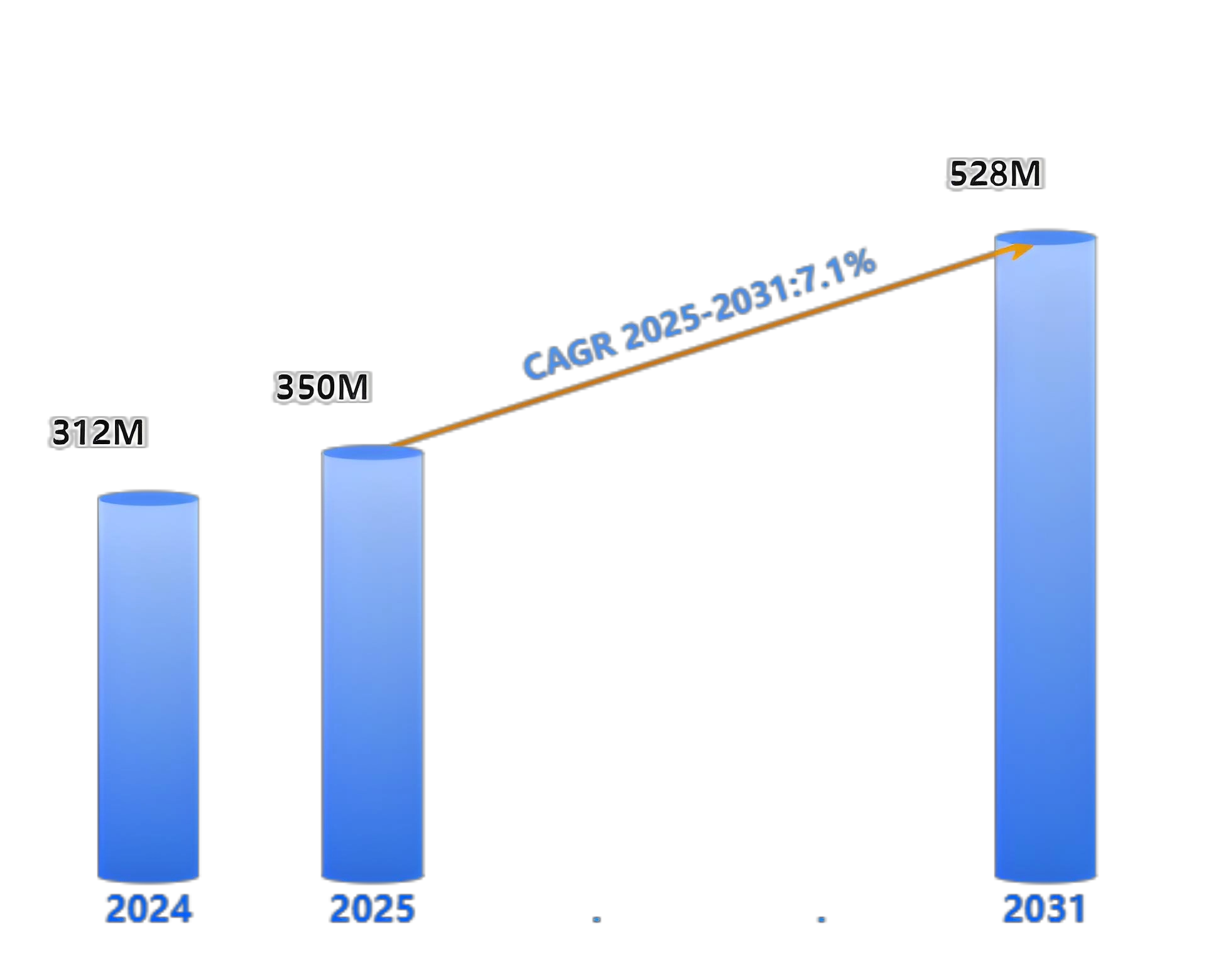
PCB는 AI 컴퓨팅 붐의 주요하고 직접적인 수혜자입니다.. 높은 성장 확실성을 제공합니다.. IEK 데이터에 따르면, 전 세계 PCB 생산량은 대략적으로 추정되었습니다. 92.36 10억 미국. 달러 2025. 이는 연간 성장률을 나타냅니다. 15.4%. 앞으로 2026, AI 인프라가 확장되면서, 전세계 PCB 시장 규모는 다음과 같이 성장할 것으로 예상됩니다. 105.2 10억 미국. 불화. 이는 성장률 13.9%. 일부 예측에 따르면 세계 PCB 시장 규모는 다음을 초과할 수 있습니다. 137.8 10억 미국. 달러 기준 2035.
우리는 이러한 성장을 세 단계로 나눌 수 있습니다:
-
단기 (2026-2027): AI 서버 볼륨 드라이버 단계. 복합 연간 성장률 (cagr) ~의 28% 에게 35%. 엔비디아 M10 등 신소재 양산으로, 고급 PCB 주문이 급증할 것입니다..
-
중기 (2028-2030): 다중 드라이버 단계. 여기에는 자동차 전자 장치와 5G 또는 6G 기술이 포함됩니다.. 예상 CAGR은 다음과 같습니다. 22% 에게 28%. 자동차 PCB 성장, ADAS 및 도메인 컨트롤러에 의해 구동, 칠 수 있다 40% 매년.
-
장기 (2030 그리고 그 이상): 전체 시나리오 침투 단계. CAGR이 이상으로 남음 18%. 세계 PCB 시장에서 중국 본토의 점유율은 다음 사이에 안정될 것으로 예상됩니다. 58% 그리고 62%.
다섯. 핵심 산업 체인 분석: 에서 “세 가지 주요 재료” 고급 제조에
AI 기반 PCB 업그레이드는 업스트림 핵심 소재에 대한 엄격한 요구로 시작됩니다.. 화진증권에 따르면, 고급 동박, 전자 천, 첨단 CCL에 필요한 특수수지도 증설 및 업그레이드 진행 중.
1. 업스트림 재료: 그만큼 “유전자” 성능 결정
-
구리 포일: 초박형 및 로우 프로파일을 향한 추세. HVLP 동박 AI 서버 CCL의 최고의 선택이 되고 있습니다. HVLP는 High Very Low Profile의 약자입니다.. 저손실 특성은 고속 전송에 필수적입니다.. 현재 고급 시장은 Mitsui Kinzoku와 같은 외국 기업이 장악하고 있습니다.. 하지만, Tongguan Copper Foil 및 Defu Technology와 같은 국내 기업이 공급망에 빠르게 진입하고 있습니다..
-
전자수지: 이는 CCL 공식에서 가장 설계하기 쉬운 부분입니다.. 보드의 유전 특성을 결정합니다., 즉 Dk와 Df. 유전 손실을 낮추기 위해, 재료는 전통적인 에폭시에서 업그레이드되고 있습니다.. 새로운 시스템에는 다음이 포함됩니다. PPO, PPE, BMI, 탄화수소 수지, 심지어 PTFE까지. Shengquan Group 및 Dongcai Technology와 같은 국내 기업은 이러한 수지의 대량 생산 및 공급을 달성했습니다..
-
유리 섬유 천: 초박형, 저유전율형으로 나아가고 있습니다.. M10 등급 처리 요구 사항을 충족하려면, 차세대 재료는 석영 섬유를 사용할 수 있습니다. 이것은 전통적인 전자 등급 유리 천을 대체합니다.. 이를 통해 신호 무결성과 안정성이 더욱 향상됩니다..
2. 미드스트림 제조: 공정 정밀도에 대한 궁극적인 테스트
고급 PCB 제조에는 많은 중요한 단계가 포함됩니다.. 여기에는 내부 레이어 이미징이 포함됩니다., 라미네이션, 교련, 도금, 및 솔더마스크 적용.
-
교련: AI 서버 PCB의 구멍 직경은 이제 미크론 수준입니다.. HDI 보드에는 다음이 필요합니다. 레이저 드릴링 기존의 기계적 드릴링 대신. 이는 고정밀 요구 사항을 충족합니다.. 이제 한씨씨앤씨 등 국내 장비업체가 이 분야를 선도하고 있다..
-
도금: 더 나은 구멍 균일성과 환경 친화성을 위해, 수직 연속 도금 (VCP) 기술은 이제 새로운 생산 라인의 주류 선택입니다.
-
주요 지표: 높은 레이어 보드를 가져 가라. 18 예를 들어 또는 더 많은 레이어. 그들의 점유율은 2.48% ~에 2024 에게 5.3% ~에 의해 2029. 이는 CAGR을 나타냅니다. 15.7% .
VI. 신뢰할 수 있는 PCB 공급업체를 선택하는 방법?
AI 파동이 치솟으면서, 기술적으로 유능하고 신뢰할 수 있는 PCB 공급업체를 선택하는 것이 중요합니다.. 이는 프로토타이핑이 필요하든 대량 생산이 필요하든 관계없이 적용됩니다.. 수많은 옵션에 직면, 이러한 점을 고려:
-
소재 인증 능력: 공급업체가 고주파 재료에 대한 소규모 배치 검증 기능을 갖추고 있습니까?? 예를 들어, M7 또는 M8 등급. 최고의 동박적층판을 추천할 수 있나요? (CCL) 당신의 특별한 디자인을 위해?
-
공정능력: 그들이 감당할 수 있을까 30 레이어? 아래의 최소 선 너비와 간격을 달성할 수 있습니까? 25 마이크로미터, 아니면 심지어 20 마이크로미터? 4차 HDI 이상을 지원할 수 있나요??
-
품질 관리: 국제 표준 인증을 받았나요?? 주요 인증에는 다음이 포함됩니다. IPC-A-600 인쇄판의 수용성을 위해. 또한, IPC-6012 견고한 인쇄 기판에 대한 자격 및 성능 사양을 다룹니다.. 엄격한 절차가 있나요? 임피던스 제어 및 신뢰성 테스트?
고급형을 찾고 계시다면 PCB 제조업체 AI 시대의 도전에 대비하다, 견적을 받아 온라인. 당신은 또한 할 수 있습니다 온라인으로 PCB 구매 요구 사항을 직접 제출하여. Shennan Circuits와 같은 주요 제조업체, WUS 인쇄 회로, 및 UGPCB는 하이엔드 HDI 및 고층 생산을 확대하고 있습니다.. 그들은 전 세계 고객에게 경쟁력 있는 솔루션을 제공하고 있습니다..
결론
NVIDIA의 M10 소재 테스트부터 천억 달러를 향한 글로벌 PCB 시장까지, 고급 제조업의 황금시대가 시작됐다. PCB는 더 이상 단순한 것이 아닙니다. “해골” 전자제품의. 그것은 “신경 센터” AI 컴퓨팅의 성공 여부 결정. 업계 전문가용, 이러한 변화를 이해하는 것이 핵심입니다. 에서 이동입니다 “규모 확장” 에게 “가치 재구성.” 이러한 이해는 향후 10년 동안 전자 산업의 흐름을 포착하는 데 필수적입니다..
