

전문가용 제품 개요: 12단 고속화, 고밀도 PCB
고속 데이터 전송과 복잡한 시스템 통합 시대, 기존의 인쇄 회로 기판 (PCB) 첨단 전자 장치의 성능 요구 사항을 충족하지 못함. 그만큼 12-레이어 고속, 고밀도 PCB 엔지니어링 솔루션입니다. 최대 특징 12 정확하게 정렬된 전도성 층, 컴팩트한 설치 공간 내에서 복잡한 상호 연결과 효율적인 신호 전송이 가능합니다., 역할을 하는 “중추신경계” 고급 네트워킹 장비용, 데이터 센터 서버, 고성능 컴퓨팅 (HPC), 그리고 AI 하드웨어.
전문가로서 PCB 제조업체 그리고 PCB 공급업체, UGPCB는 고급 프로세스를 활용하여 안정적인 서비스를 제공합니다. 12-층 PCB 보드 생산, 귀하의 제품이 경쟁력 있는 성능 우위를 유지하도록 보장.
심층 매개변수 분석: 성과의 기초
고품질의 능력 다층 인쇄 회로 보드 사양에 따라 정의됩니다.. 아래는 이 제품의 핵심 매개변수에 대한 분석입니다.:
-
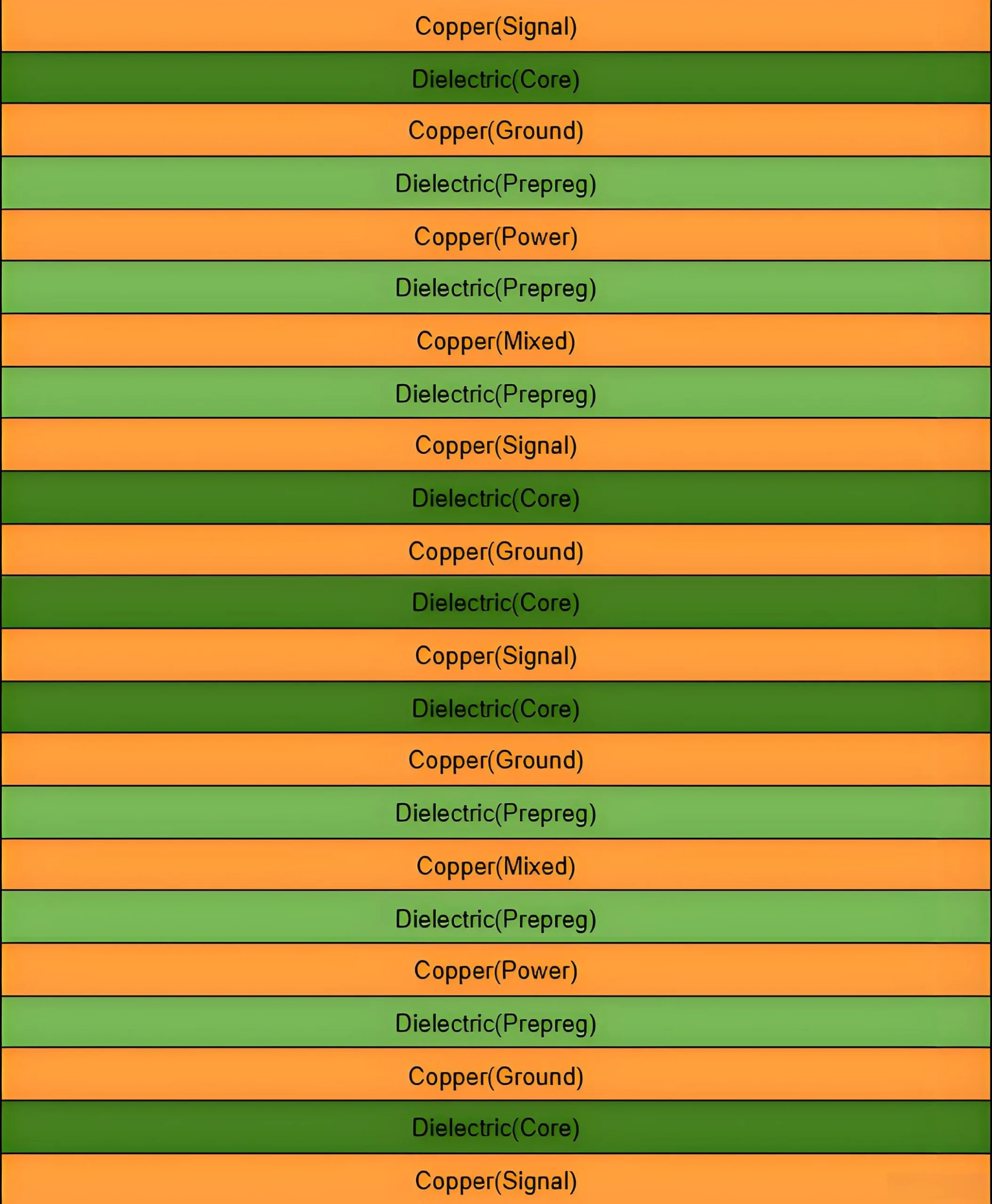
레이어 수 & 스택업: 12 레이어. 이것 다층 PCB 설계 탁월한 신호 무결성 제공 (그리고), 전력 무결성 (PI), 레이어 수가 적은 보드에 비해 EMC 성능. 전용 전원 및 접지면을 허용합니다., 고속 신호에 대한 명확한 복귀 경로 제공.
-
보드 두께 & 용인: 2.4mm ±10%. 이 견고한 두께는 백플레인 및 대형 폼 팩터 애플리케이션에 탁월한 기계적 강도를 제공합니다., 결합 및 설치 중 신뢰성 보장. 엄격한 공차로 인해 조립의 일관성이 보장됩니다..
-
완성되는 구리 무게: 고유한 배포:
1/1/1/1/1/2/2/1/1/1/1/1 oz. 이는 내부 레이어를 나타냅니다. (L6 & L7) 2온스 무거운 구리를 활용, 고전류 전력 공급을 위해 특별히 설계됨. 외부 및 기타 신호 레이어는 1oz 구리를 사용합니다., Fine-line Etching에 최적화. 이 하이브리드 구조는 높은 신뢰성 PCB 제작. -
중요한 프로세스 기능:
-
최소 드릴 구멍 크기: 0.2mm. 고밀도 BGA 팬아웃 지원, 라우팅 유연성 향상.
-
최소 라인 너비/공간: 0.076mm / 0.09mm (3밀 / 3.5밀). 달성 고밀도 상호 연결 (HDI)-레벨 라우팅, 고속 신호 전파에 필수적인.
-
-
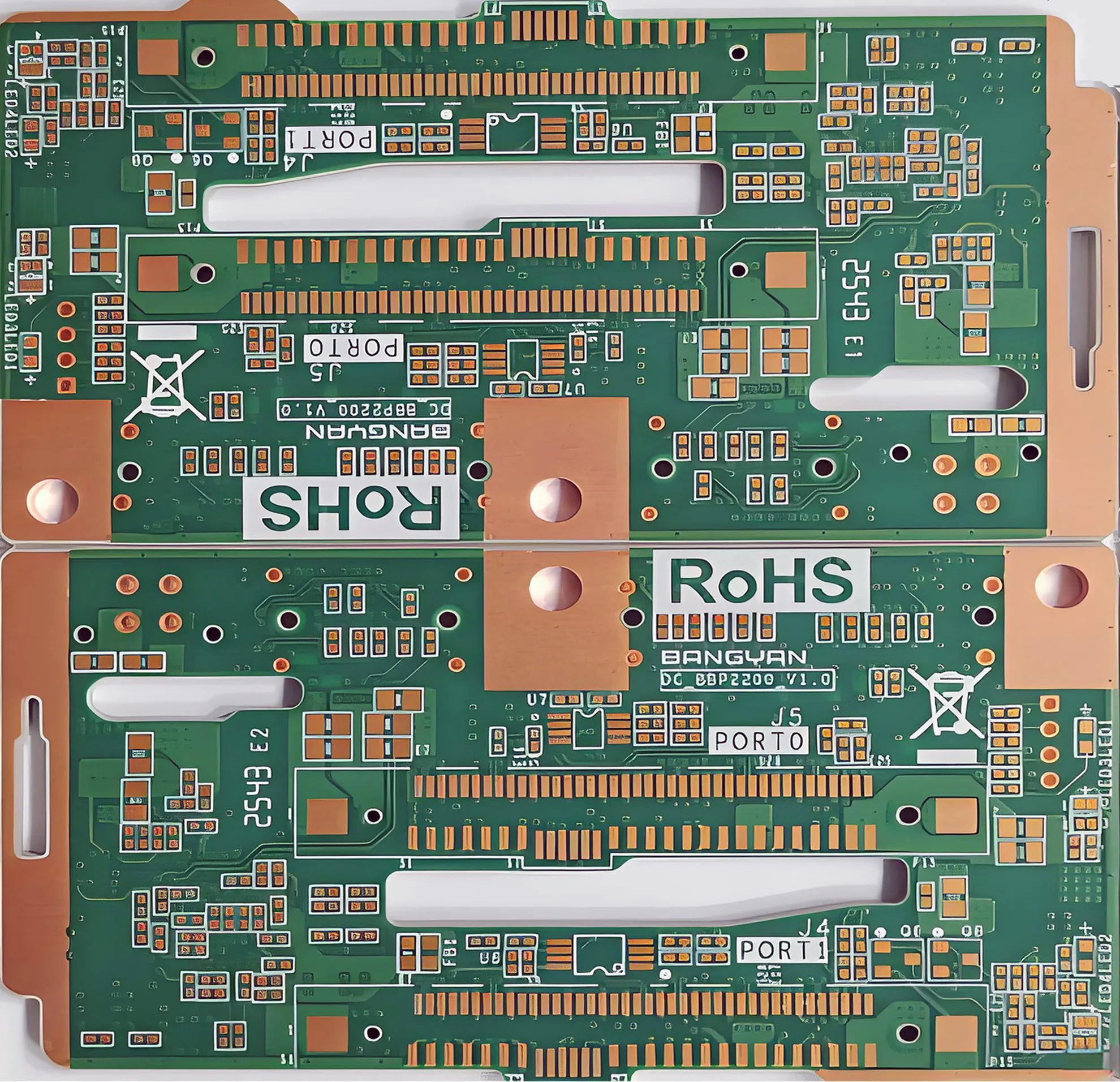
표면 마감: OSP (유기 용해성 보존). 납 함유 및 무연 납땜 모두와 호환 가능, 구리 패드를 산화로부터 보호합니다., 우수한 표면 평탄성을 제공합니다., 비용 효율적입니다. 밀도가 높은 SMT가 있는 보드에 이상적입니다. 구성 요소.
핵심 재료 & 핵심기술: 탁월한 신호 무결성 구현
-
고성능 라미네이트: 활용 난야 NY6300S 고속 라미네이트. 높은 유리 전이 온도 (Tg >150℃) 고온 리플로우 솔더링 중 치수 안정성과 신뢰성 보장. 최적화된 유전 상수 (DK) 및 소산 인자 (Df) 고주파수에서 신호 손실을 크게 줄입니다., 물질적 기반을 형성하다 고주파 PCB.
-
고급 구리 포일: 고용 RTF (역방향 처리 포일) 구리. 표준 전착과 비교 (에드) 박, RTF 포일은 더 부드러운 특징을 가지고 있습니다., 처리된 면의 낮은 프로파일 표면. 이로 인해 신호 손실이 줄어듭니다. “피부 효과” 높은 주파수에서, 다음을 초과하는 차동 신호의 성능을 크게 향상시킵니다. 10 Gbps.
-
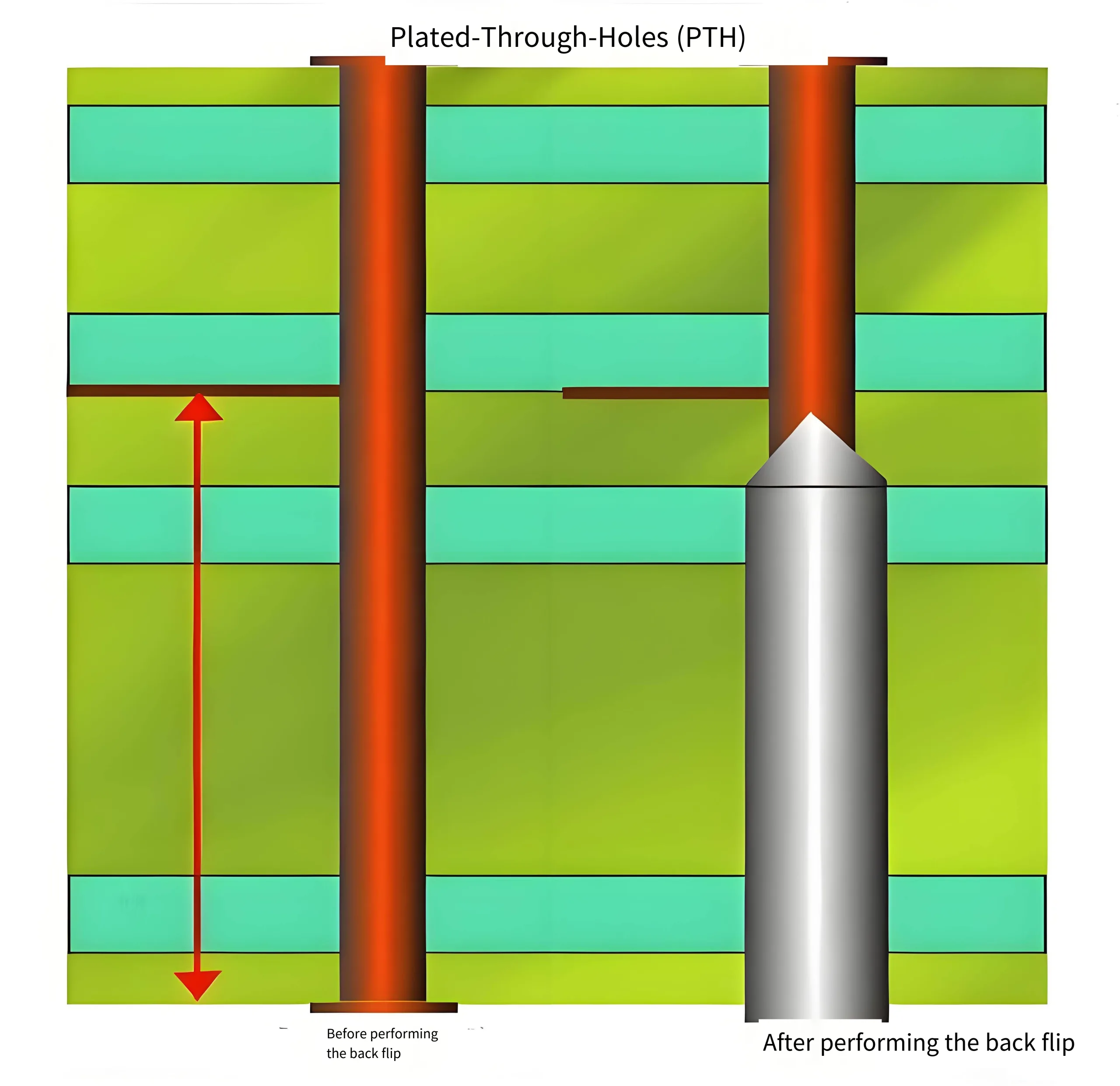
중요한 프로세스: 제어된 깊이 드릴링 (후면 드릴링): 12층 이상 다층 PCB, 사용하지 않은 부분 (그루터기) 스루홀 비아는 상당한 신호 반사를 일으킬 수 있습니다., 품위를 떨어뜨리는. 그만큼 백 드릴링 공정 스텁을 통해 이 비기능적 요소를 정확하게 제거합니다., 부정적인 영향을 제거하는 핵심 기술입니다. 고속 다층 PCB 성능.
생산 흐름 & 품질 보증
UGPCB 12-레이어 PCB 제조 공정 엄격히 준수한다 IPC 표준 그리고 다음을 포함합니다 제조 가능성을위한 설계 (DFM) 검토, 내부 레이어 이미징, 라미네이션, 교련 (백 드릴링 포함), 도금, 외부 레이어 이미징, 솔더 마스크 적용, 표면 마감 (OSP), 라우팅, 전기 테스트, 및 최종 검사. 각 단계는 정밀 측정 장비로 지원됩니다. (AOI, 임피던스 테스트, 플라잉 프로브 테스트), 모든 것을 보장 회로 기판 제공되는 제품은 설계 사양과 당사의 고품질 표준을 충족합니다..
일반적인 응용 프로그램 & 제품 분류
이 고성능 PCB 보드 까다로운 전기 환경과 복잡한 시스템을 위해 설계되었습니다., 주로 사용되는:
-
하이엔드 네트워크 & 통신 장비: 400G/800G 광 모듈용 코어 마더보드, 고급 라우터, 그리고 스위치.
-
데이터 센터 & 클라우드 컴퓨팅: 서버 마더보드, 가속기 카드, 스토리지 백플레인.
-
고성능 컴퓨팅: 워크스테이션 마더보드, GPU 컴퓨팅 카드, AI 가속기 하드웨어.
-
고급 테스트 & 측정 장비: 초고주파 신호를 처리하는 장비용 내부 보드.
과학적인 제품 분류:
-
레이어 수에 의해: 다층 PCB (>8 레이어)
-
기술 유형별: 고속/고주파 PCB, HDI PCB, 무거운 구리 PCB (부분적인)
-
응용 프로그램에 의해: 통신 인프라 PCB, 데이터센터/서버 PCB
12층 고속 PCB에 UGPCB를 선택하는 이유?
-
기술 전문 지식: 입증된 숙달 백 드릴링 그리고 RTF 구리박 고속 설계 과제를 해결하기 위한 애플리케이션.
-
정밀가공: 가능 3/3.5 밀 라인/스페이스, 엄격한 고밀도 상호 연결 요구 사항 충족.
-
재료 무결성: 평판의 핵심 사용 고속 라미네이트 Nanya NY6300S와 마찬가지로 기본 성능을 보장합니다..
-
설계 지원: 전문가 PCB 설계 그리고 DFM 검토 프로젝트 시작부터 위험을 제거하는 서비스.
-
일관된 품질: 완전히 통제되는 PCB 생산 검사 시스템을 통해 신뢰할 수 있는 제품을 제공합니다..
하드웨어를 향상할 준비가 되었습니다.? UGPCB 엔지니어에게 문의하세요. 무료 PCB 견적 그리고 DFM 분석 다음 12단 고속 보드 프로젝트에.


이 인터넷 웹사이트는 이와 관련하여 귀하가 원했던 데이터를 안내하는 것일 수 있지만 누가 해야 할지 몰랐습니다.. 여기를 잠깐 살펴보세요, 그리고 당신은 그것을 완전히 발견하게 될 것입니다.