

무엇입니까? 4 레이어 PCB?
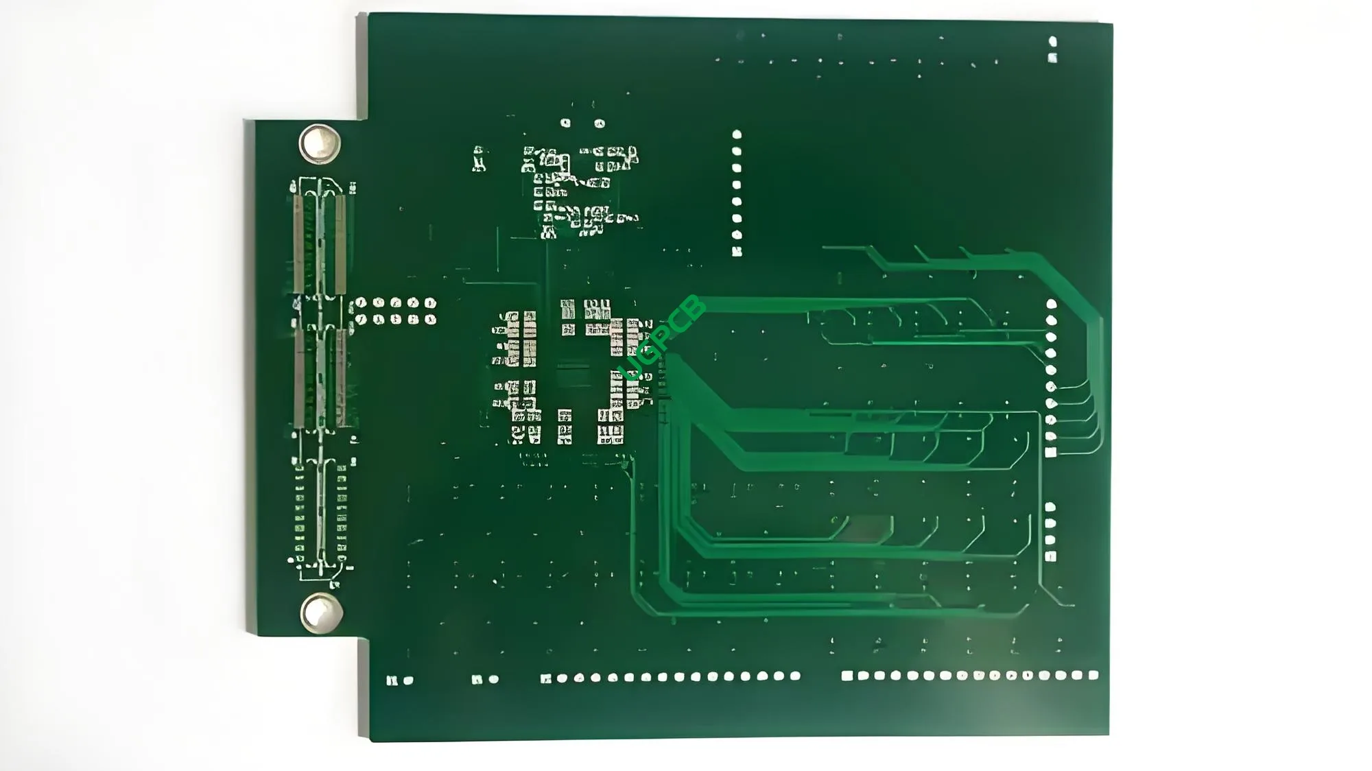
A 4-layer Printed Circuit Board (PCB) is an advanced 전자 구성 요소 that consists of four layers of conductive material, 일반적으로 구리, 절연 층으로 분리됩니다. This multilayer structure allows for complex circuit designs with high density and improved performance.
설계 요구 사항
Designing a 4-layer PCB involves several key considerations:
- 재료: Commonly made from FR-4, a composite material known for its excellent electrical properties and affordability.
- 레이어 수: 이름에서 알 수 있듯이, it has four layers, which can handle more complex circuitry compared to single or double-sided boards.
- 구리 두께: Can range from 0.5OZ to 6OZ, depending on the application’s power requirements.
- 표면 처리: Options include immersion gold, OSP (유기 용해성 보존), and lead-free HASL (Heat Activated Solder Leveling), each offering different levels of solderability and protection.
- 추적과 공간: Minimum trace and space are typically set at 3mil (0.075mm), allowing for fine details in the circuit design.
어떻게 작동하나요??
The 4-layer PCB functions by providing a platform where electronic components can be mounted and interconnected using conductive pathways etched into the copper layers. These pathways are separated by insulating layers, preventing electrical shorts while allowing signals to pass through via plated through-holes or vias.
응용
복잡성과 신뢰성으로 인해, 4-층 PCB are widely used in various consumer electronics including:
- 스마트폰
- 정제
- 노트북
- Gaming consoles
- High-end audio equipment

분류
4-layer PCBs can be classified based on several factors:
- 재료로: Most commonly made from FR-4 due to its balance of cost, 힘, 및 전기 특성.
- 구리 두께별: 경량부터 다양함 (0.5온스) 헤비급으로 (6온스) 애플리케이션의 필요에 따라.
- 표면 처리에 의한: Options include immersion gold, OSP, and lead-free HASL, each offering different levels of protection and solderability.
사용된 재료
The primary materials used in manufacturing 4-layer PCBs include:
- FR-4: 우수한 기계적 강도와 열적 안정성을 제공하는 유리 강화 에폭시 적층판.
- 구리: 전도층에 사용, 설계 요구 사항에 따라 두께가 다양함.
- 솔더 마스크: Typically green, 하얀색, 빨간색, or black, 산화 및 우발적인 단락으로부터 구리 트레이스를 보호합니다..
- Surface Treatments: Such as immersion gold, OSP, or lead-free HASL, which improve solderability and protect against corrosion.
성능 특성
Key performance attributes of a 4-layer PCB include:
- 고밀도: 더 많은 것을 허용합니다 구성 요소 더 작은 공간에 포장하기 위해.
- 신뢰할 수 있음: 여러 레이어를 사용하면 전기 단락 위험이 줄어들고 신호 무결성이 향상됩니다..
- 신호 무결성: 더 짧은 신호 경로와 감소된 누화로 인해 개선됨.
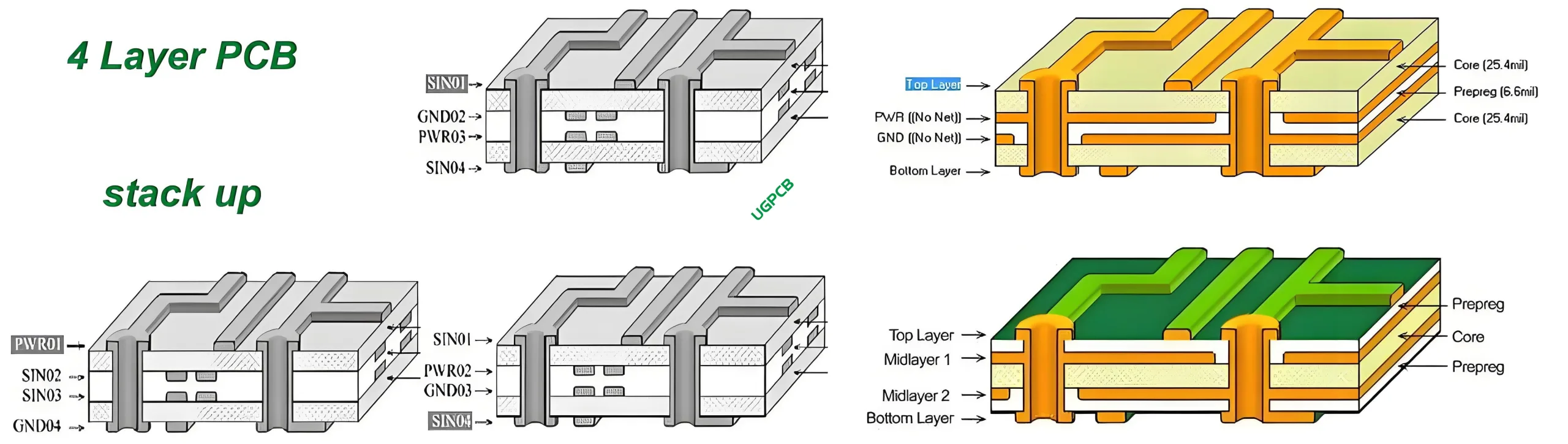
구조적 구성
구조적으로, a 4-layer PCB comprises:
- 전도성 층: 구리로 만든, 원하는 회로 패턴으로 에칭.
- 절연층: 전도성 층 사이의 전기적 단락 방지.
- 도금된 스루홀 비아: 서로 다른 레이어 간의 연결을 촉진합니다..
독특한 특징
Some notable features of a 4-layer PCB are:
- 파인 피치: Allows for high-density interconnects, making it ideal for compact devices.
- 견고성: 여러 레이어를 사용하면 보드와 구성 요소 사이에 강력한 기계적 결합이 제공됩니다..
- 다재: 사용자 정의 가능한 레이어 수 및 재료 선택으로 인해 광범위한 응용 분야에 적합합니다..
생산 과정
The manufacturing process of a 4-layer PCB involves several steps:
- 디자인 및 레이아웃: 전문 소프트웨어를 사용하여 회로 패턴 생성.
- 재료 준비: 기본 재료를 크기에 맞게 절단하고 표면을 청소합니다..
- 라미네이션: 열과 압력을 가해 개별 레이어를 적층하고 접착.
- 에칭: 원하는 회로 경로를 형성하기 위해 과도한 구리를 제거합니다..
- 도금: 비아와 노출된 구리 영역에 얇은 금속층 추가.
- 솔더 마스크 적용: Applying the green, 하얀색, 빨간색, or black coating to protect traces.
- 표면 처리: Applying immersion gold, OSP, or lead-free HASL for solderability.
- 최종검사: 배송 전 품질과 기능성 보장.
사용 사례
Common scenarios where a 4-layer PCB might be employed include:
- High-density interconnect applications in mobile devices.
- 낮은 신호 손실이 요구되는 고급 통신 시스템.
- 열악한 환경에서 안정적인 성능이 필요한 휴대용 의료 기기.
- 견고성과 수명을 요구하는 자동차 전자 장치.
요약하면, the 4-layer PCB represents a significant advancement in 인쇄 회로 기판 기술, offering unparalleled complexity and performance for modern electronic applications. Its design flexibility combined with superior signal integrity and durability makes it an essential component in the development of next-generation consumer electronics and beyond.


