
Product Overview and Core Parameters
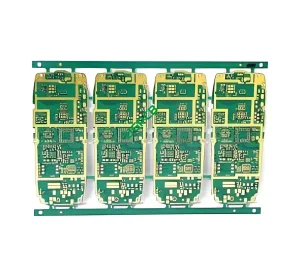
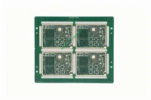
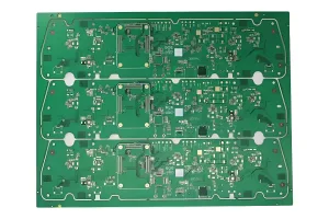
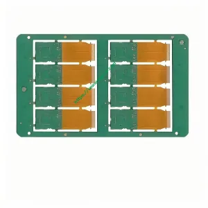
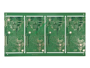
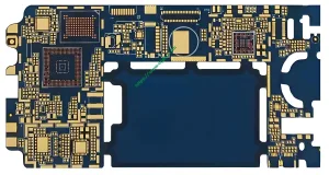
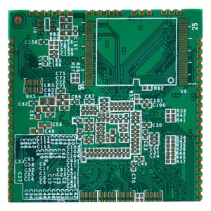
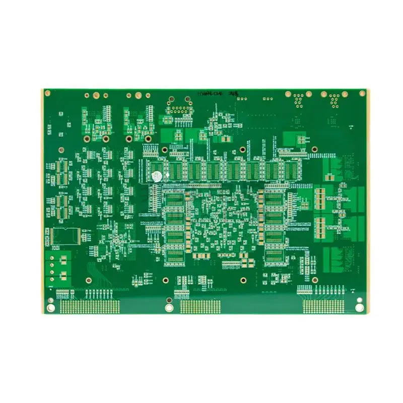
UGPCB builds the 6L 2+N+2 HDI WiFi Module PCB for WiFi 6, WiFi 6E, and WiFi 7 radio modules. It uses a 6-layer, 2+n+2 HDI 스택 up. The board uses FR4 Tg170 material. Finished thickness is 0.8mm. Copper thickness is 1OZ. Minimum trace and space are 3mil/3mil. Minimum laser hole is 0.1mm. Surface finish is immersion gold plus OSP. Solder mask color options are black and white. 이것 HDI PCB supports fine-pitch BGA fanout for WiFi RF chips.
| 매개 변수 | 사양 |
|---|---|
| 레이어 | 6 레이어 |
| 건설 | 2+N+2 HDI (2+2+2 build-up) |
| 재료 | FR4 Tg170 |
| 완성된 두께 | 0.8mm |
| 구리 두께 | 1온스 (35μm) |
| 색상 | 검은색 / 하얀색 |
| 표면 처리 | 이머젼 골드 + OSP |
| 최소 추적 / 공간 | 3밀 / 3밀 (about 0.076mm) |
| Min Laser Hole | 0.1mm |
| 애플리케이션 | Wi -Fi 모듈 PCB |

What Is an HDI PCB and a 2+N+2 Stackup?
HDI PCB means high-density interconnect printed circuit board. It uses microvias, 묻힌 vias, and fine traces. These features increase routing density. IPC-2226 defines HDI stackup types. A 2+N+2 structure is a two-level build-up. It adds two build-up layers on each side of the core. For a 6-layer board, the stack is L1-L2, L3-L4, and L5-L6. Laser microvias connect L1-L2, L2-L3, L4-L5, and L5-L6. Buried vias connect L3-L4. This construction supports 0.4mm to 0.5mm pitch BGA fanout.
Design Guidelines for WiFi Module PCB
RF Impedance Control
WiFi modules need stable 50Ω RF traces. Trace width, 갭, 유전 상수, and ground reference set the impedance. Texas Instruments recommends 50Ω RF traces and a solid ground reference. It also recommends a pi matching network at the antenna. Avoid 90-degree bends in RF traces. Use smooth curves instead. UGPCB controls 3mil/3mil traces and 에프R4 Tg170 유전체 특성. These features help maintain impedance consistency.
Material Selection and High-Frequency Performance
WiFi 6E adds the 6GHz band from 5.925GHz to 7.125GHz. Standard FR4 has a dissipation factor near 0.020. At 6GHz, this loss can reduce link budget. FR4 Tg170 offers better thermal stability than standard FR4. Its Tg is 170°C. It survives lead-free soldering above 260°C. For higher frequency needs, UGPCB can use Rogers RO4350B in a hybrid stackup. This option lowers RF loss while controlling cost.
BGA Fanout and Routing Density
Modern WiFi chips use fine-pitch BGA or QFN packages. Pitch can reach 0.4mm. The 2+N+2 HDI structure routes traces through laser microvias. This approach frees surface area. 결과적으로, it solves routing congestion on traditional through-hole PCBs.
작동 원리 및 전기적 성능
HDI PCB performance comes from its build-up structure. Microvias replace mechanical through holes. They shorten layer-to-layer paths. They also reduce parasitic inductance and capacitance. Lower parasitics help GHz RF signals. A 1OZ copper layer supports power and ground planes. IPC-2221 provides design charts for trace width and current capacity. The 3mil/3mil line width supports differential pairs and impedance-matched traces. This capability matters for WiFi 6E and WiFi 7 PCB 디자인.
Production Process and Manufacturing
UGPCB uses multiple lamination, 레이저 드릴링, and plating steps.
- Inner-layer imaging and core lamination: We image and etch inner layers. We then vacuum laminate cores. We form buried vias before core lamination.
- First sequential lamination: We add one dielectric layer and copper foil on each side. We then laser-drill L2-L3 and L4-L5 microvias at 0.1mm.
- Second sequential lamination: We add another dielectric layer and copper foil. We then form L1-L2 and L5-L6 microvias.
- Outer-layer imaging and surface finish: We etch outer traces. We print black or white solder mask. We apply immersion gold plus OSP.
- Electrical test and inspection: 우리는 공연한다 100% 전기 테스트. We also run cross-section analysis and thermal stress tests.

Quality Control and Reliability Standards
IPC-6012F covers rigid PCB qualification and performance. It defines Class 1, 수업 2, 그리고 수업 3. UGPCB recommends Class 2 for WiFi module PCB. For plated through holes, 수업 2 requires 20µm average copper. 수업 3 requires 25µm average copper. For industrial or automotive WiFi modules, 수업 3 offers higher reliability. IPC-6012F also addresses stacked microvia reliability. UGPCB uses AOI after laser drilling. We verify copper thickness with cross sections. We run thermal stress tests at 288°C for 10 초. We also use tdr to check 50Ω impedance within ±10%.
Applications and Market Value
일반적인 응용 프로그램
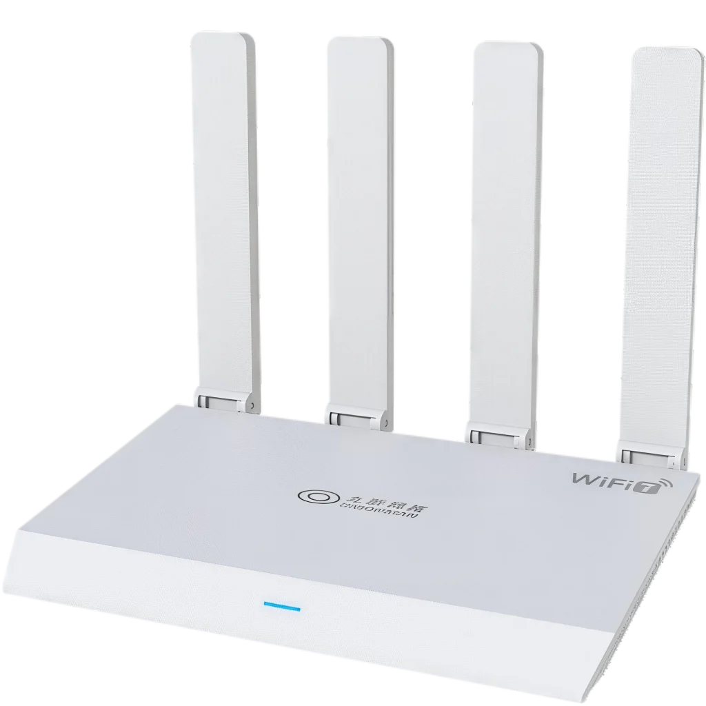
- WiFi 6, WiFi 6E, and WiFi 7 router modules
- IoT gateways for smart home and industrial IoT
- 5G CPE terminals
- Automotive WiFi hotspot modules
시장 동향
Prismark reports strong HDI PCB growth in 2025. HDI output value grew 25.6% year over year. Prismark projects an 11.2% CAGR from 2024 에게 2029. AI infrastructure and high-speed networks drive this growth. WiFi 6E and WiFi 7 adoption also increases demand for high-frequency HDI PCB. Manufacturers with 3mil/3mil lines and 0.1mm laser vias will gain an edge.
Why Choose UGPCB for Your HDI WiFi Module PCB?
- Proven HDI manufacturing: UGPCB produces 2+N+2 HDI PCB in volume. We achieve 3mil/3mil trace and space. We also achieve 0.1mm laser holes.
- Strict quality control: We build to IPC-6012 Class 2. We provide cross-section reports and test data.
- Optimized materials: FR4 Tg170 balances thermal stability and cost. We also offer Rogers hybrid stackups for higher frequencies.
- 엔지니어링 지원: We support stackup design, impedance simulation, and DFM review. This support shortens your development cycle.
- PCB assembly option: UGPCB also offers PCB services for WiFi modules. We can source components and assemble boards.
Contact UGPCB today for a quote. Our engineering team will reply within 24 시간. We will provide stackup advice and sample support.
데이터 소스 설명
This article cites the following standards and sources.
- IPC-2226, Sectional Design Standard for High Density Interconnect (HDI) 인쇄보드. It defines HDI stackup types, including 2+N+2.
- IPC-6012F, 경질 인쇄 기판의 자격 및 성능 사양, 십월 2023. It defines Class 1, 수업 2, 그리고 수업 3 요구 사항.
- IPC-2221, 인쇄 기판 설계에 대한 일반 표준. It provides trace width and current capacity guidance.
- Prismark Partners, HDI PCB market statistics and forecast, 2025.
- Texas Instruments, SimpleLink™ Wi-Fi® Layout Guidelines. It specifies 50Ω RF traces and pi matching networks.
We checked all data and formulas in this article. We found no errors in the cited values.