
In the era of high-speed data transfer and precision computing, the performance of the 인쇄 회로 기판 (PCB)—the core brain of electronic devices—determines the entire system’s capability. UGPCB introduces its high-performance 18-레이어 견고한 PCB 기반으로 Megtron-7 재료, engineered to meet the most demanding electrical and physical challenges, serving as the essential foundation for your next-generation advanced equipment.
1.18-Layer Megtron-7 Rigid PCB 제품개요 & 정의
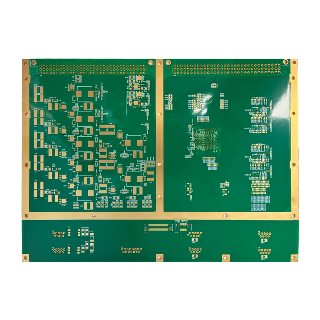
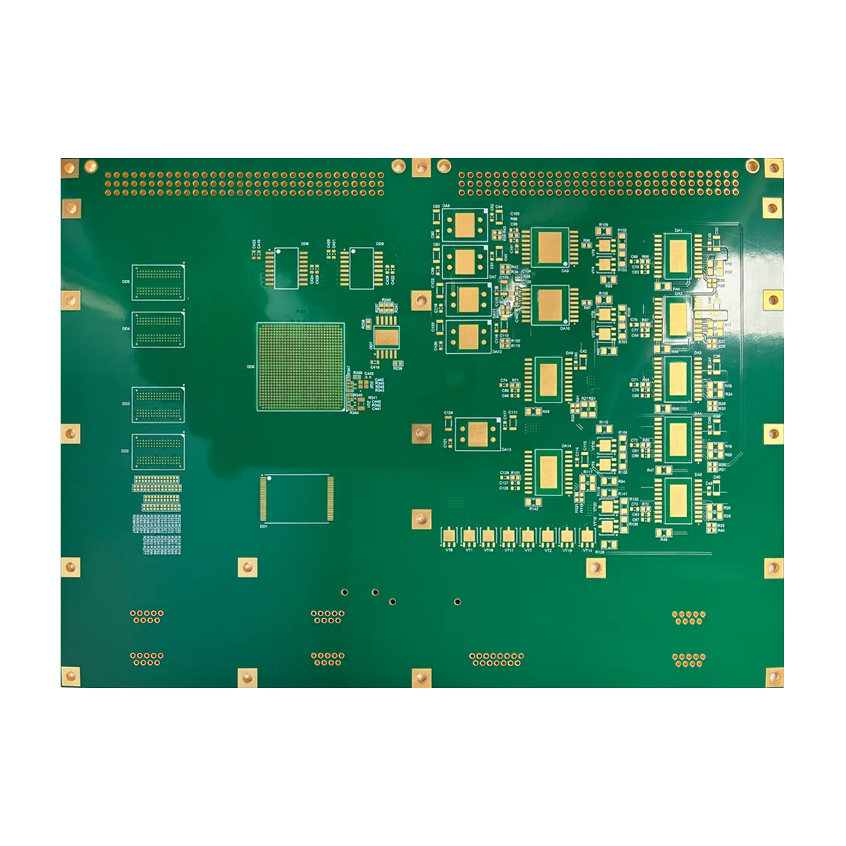
This product is an 18-layer rigid high-layer count PCB with a precisely controlled thickness of 1.86mm and overall dimensions of 165mm x 120mm. It utilizes industry-leading Megtron-7 high-speed low-loss laminate and features a 2-microinch (대략. 0.05μm) 무전해 니켈 침지 금 (동의하다) 표면 마감. This specification represents an advanced tier in 고성능 PCB 제조, designed for applications where signal integrity, 열 관리, and reliability are paramount.
2. 중요한 설계 고려 사항
Designing a successful 18-layer PCB, especially with high-speed materials like Megtron-7, requires careful attention to several core aspects:
-
스택업 디자인: A rational layer stack-up is critical for impedance control and crosstalk reduction. A typical 18-layer stack includes multiple signal, 힘, and ground planes to ensure stable power distribution and clear signal return paths.
-
임피던스 제어: High-speed signal transmission demands precise 제어된 임피던스 PCB 설계. Trace width and spacing must be calculated accurately based on the Dk (유전 상수) 및 Df (소산 인자) of Megtron-7. We offer professional impedance calculation and simulation services.
-
열 관리: The 1.86mm board thickness and multi-layer structure necessitate effective thermal pathways in the design, such as using thermal vias to connect internal copper layers for efficient heat dissipation from components.
-
고밀도 상호 연결 (HDI) Considerations: While this is a standard through-hole design, careful planning of via types (blind, 매장, through-hole) is essential at this layer count to minimize stub effects and optimize signal paths.
3. 작동 방식 & 구조
에이 다층 PCB functions like a highly integrated, three-dimensional “road network.” Electrical signals travel on copper traces (“roads”) on the surface and internal layers, with vertical connections between layers established through plated through-holes (“interchanges”). Dedicated power and ground planes provide stable voltage reference and noise shielding for the entire system. 이것 18-레이어 견고한 PCB is formed through a precise lamination process, bonding multiple core layers and prepreg sheets into a single, robust unit with excellent electrical properties. Its sophisticated PCB board structure is the foundation for implementing complex circuit functionalities.
4. 핵심 재료 & 주요 성과
-
사용된 재료:
-
라미네이트: Megtron-7. This is a high-performance, low-loss copper-clad laminate from Panasonic, renowned for its stable dielectric constant (Dk ~3.3) and extremely low dissipation factor (Df ~0.001). It is optimized for applications above 10GHz and into millimeter-wave frequencies.
-
구리 포일: Utilizes Very Low Profile (VLP) or Reverse Treated Foil (RTF) to minimize “피부 효과” losses caused by signal transmission on rough copper surfaces.
-
표면 마감: 무전해 니켈 침지 금 (동의하다, 2유”). Provides a flat surface, 우수한 납땜성, 안정적인 접촉 인터페이스 (suitable for gold fingers), 그리고 긴 유통기한.
-
-
Outstanding Performance:
-
탁월한 신호 무결성 (그리고): Exceptionally low signal loss ensures high-speed pulse waveforms remain undistorted.
-
Excellent Power Integrity (PI): Multiple dedicated power and ground planes offer very low power distribution network impedance and superior decoupling.
-
높은 신뢰성: The 1.86mm board thickness and premium materials deliver high mechanical strength, 내열, and long-term environmental stability.
-
Stable Impedance Control: Achieved through material consistency and precision manufacturing processes.
-
5. 제품 분류
According to industry and IPC standards, this product is accurately classified as:
-
레이어 수에 의해: High-Layer Count PCB (typically defined as 10+ 레이어).
-
재료 유형별: High-Speed High-Frequency PCB / 저손실 PCB.
-
구조 별: 강성 PCB.
-
기술 별: Controlled Impedance PCB, ENIG Finished PCB.
-
By Application Grade: Industrial Grade / Telecommunications Grade High-Performance PCB.
6. 주요 특징 & 이익
-
Premium Material: 기반 Megtron-7 high-speed laminate, providing the physical basis for superior electrical performance.
-
High Complexity Capacity: 그만큼 18-layer circuit board design allows for extremely complex and dense circuit layouts.
-
정밀가공: Strict tolerance control on the 1.86mm board thickness and consistent 2유” 동의하다 surface finish application.
-
Engineered for Speed: Optimized throughout—from design and material selection to processing—for 고속 디지털 회로 그리고 RF/microwave circuits.
7. 생산 공정 개요
그만큼 high-layer count PCB manufacturing process is highly precise: Material Cutting → Inner Layer Imaging & Etching → Automated Optical Inspection (AOI) → Lamination (Pressing multiple inner layer cores with prepreg) → Drilling → Hole Metallization (desmear, Electroless & Electrolytic Copper Plating) → Outer Layer Imaging → Pattern Plating → Etching → Solder Mask Application → Surface Finish (동의하다) → Profile Routing → Electrical Testing → Final Inspection. Each step requires stringent control, particularly layer-to-layer registration and impedance control.
8. 기본 응용 프로그램 & 사용 사례
이것 high-performance PCB board is the ideal choice for the following advanced applications:
-
High-Speed Communication Equipment: 400G/800G 광 모듈용 코어 마더보드, 고급 라우터, 그리고 스위치.
-
고급 컴퓨팅 & 저장: 서버 마더보드, AI 가속기 카드, high-speed storage array (SSD) controller boards.
-
Precision Test & 측정 장비: Internal core boards for high-end oscilloscopes, 스펙트럼 분석기, 및 신호 발생기.
-
항공우주 & Defense Electronics: Processing units within radar systems and satellite communication payloads.
-
Advanced Medical Imaging Devices: High-speed data acquisition and processing boards for equipment like MRI and CT scanners.

Why Choose UGPCB for Your 18-Layer Megtron-7 PCBs?
We deliver more than just a 회로 기판; we provide a complete solution encompassing DFM (제조 가능성을위한 설계) 검토, 정밀 제조, 그리고 신뢰성 테스트. We possess deep expertise in every detail of 높은 레이어 수 PCB 제작, ensuring your design is translated into reality with the highest quality and reliability.
오늘 저희에게 연락하세요 for a free technical assessment and a competitive quote for your project. Let UGPCB be the robust foundation for your high-end product’s success.


