
Power the Future of Computing: UGPCB’s High-Performance Server PCB Solutions
In today’s rapidly evolving landscape of data centers, 인공지능, 그리고 클라우드 컴퓨팅, server performance and stability are pivotal to digital efficiency. As the fundamental hardware bedrock, the quality of Server 인쇄 회로 기판 (PCB) 가장 중요하다. Leveraging deep technical expertise, UGPCB는 전문적인, customized, high-performance server PCB manufacturing and PCB (인쇄 회로 보드 어셈블리) one-stop solutions.
1. 제품개요 & 정의
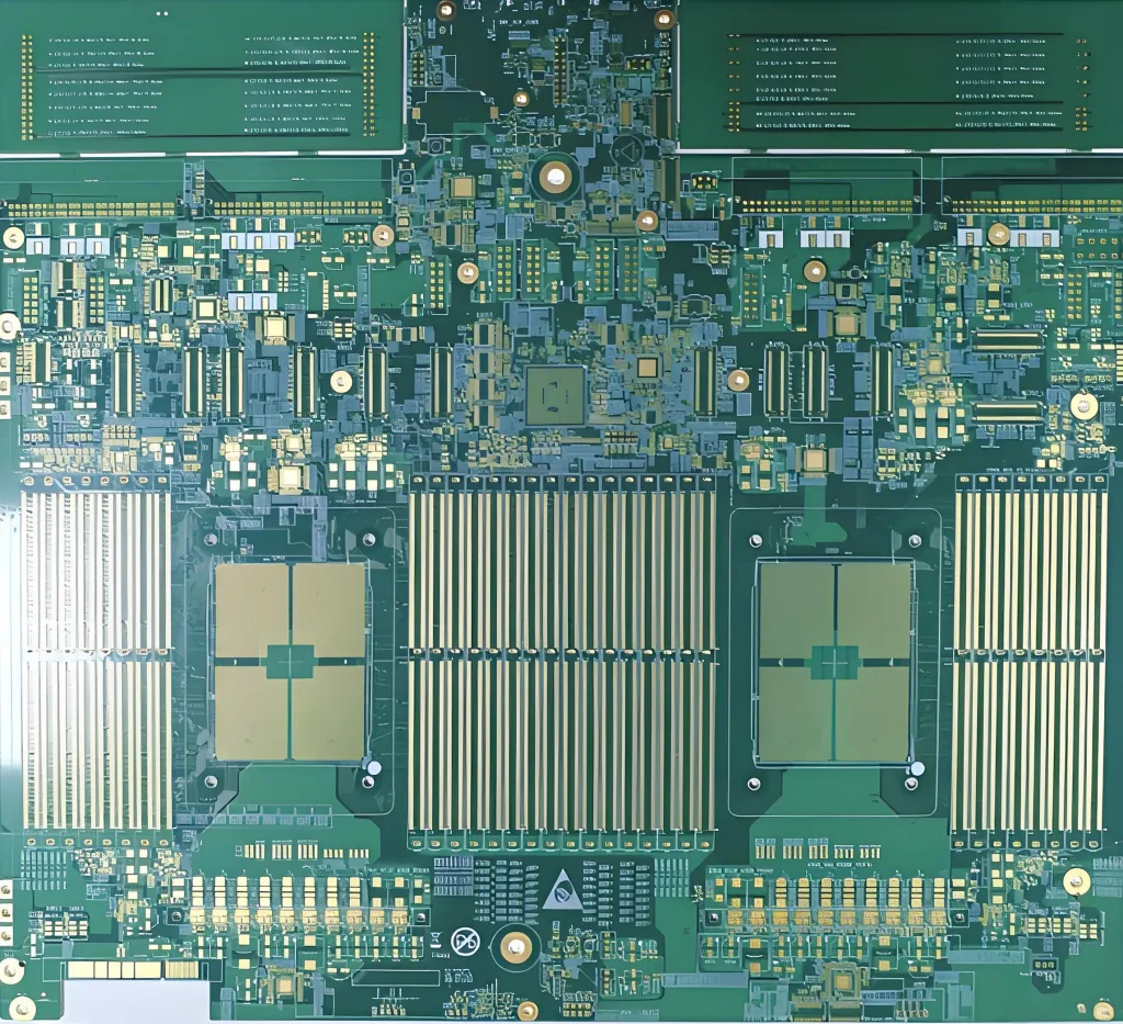
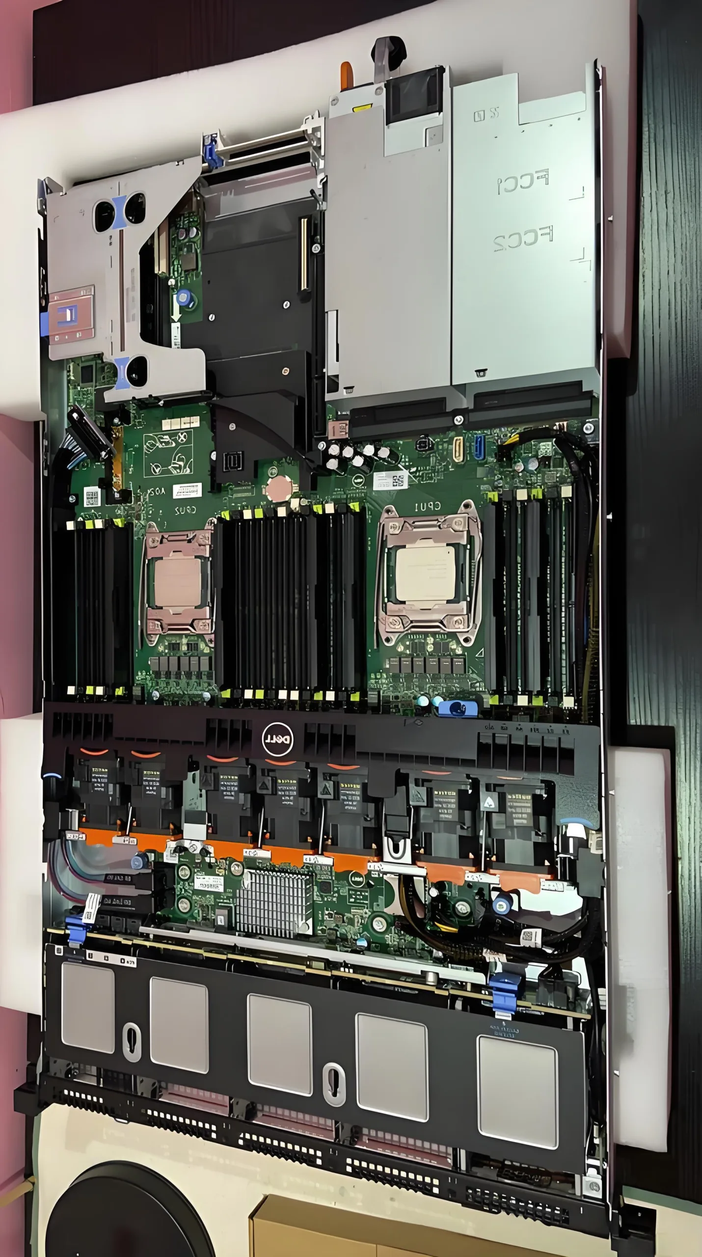
A Server PCB is a complex, multi-layer circuit board specifically engineered for server-class products. Its critical mission is to host core components like CPUs, 메모리, high-speed buses, and power modules while ensuring stable signal transmission at speeds of tens of Gbps and beyond. It is not merely a physical connection platform but the core element guaranteeing the system’s signal integrity, 전력 무결성, and thermal performance.
The specifications you provide (보드 두께: 2.8mm ±10%, 22 레이어, 2/1 oz Copper Weight, 0.1/0.1 mm Trace/Space) define a typical high-layer-count, 고밀도, high-speed server PCB. It is suitable for critical applications in mid-to-high-end dual-processor or AI server motherboards, accelerator cards, and backplanes.

2. 디자인 필수사항 & Key Technologies
The success of such advanced PCB 디자인 hinges on mastering a range of cutting-edge technologies:
-
스택업 & 임피던스 제어: The complex 22-layer stack-up requires precise calculation to achieve strict 임피던스 제어 (typically 50Ω single-ended, 100Ω 차동), forming the cornerstone of 고속 PCB 설계.
-
후면 드릴링: This critical process removes the unused copper stub from high-speed signal vias (예를 들어, for PCIe, DDR buses), 신호 반사 및 감쇠를 크게 줄입니다., and is central to enhancing signal integrity.
-
High-Speed Laminate Application: We utilize premium high-speed materials like IT-968G & IT-180A from ITEQ. Their low dissipation factor (Df) and stable dielectric constant (DK) ensure signal purity and low latency. A high Glass Transition Temperature (Tg >170℃) guarantees material reliability under the prolonged high-temperature operation of servers.
-
RTF (Reverse Treated Foil) 구리: Its smoother surface profile effectively reduces “피부 효과” losses for high-frequency signals on the conductor surface, further enhancing high-speed performance.
-
Any-Layer HDI & Hybrid Construction: Supports high-density routing. Combined with hybrid construction techniques, it allows the use of different performance materials in localized areas (예를 들어, high-current power zones vs. high-speed signal zones) to meet specific circuit requirements.
3. 성능 & 구조적 특징
-
탁월한 전기적 성능: Extremely low signal loss and excellent impedance consistency meet the demands of high-speed protocols like PCIe 4.0/5.0 and DDR4/DDR5.
-
Ultra-High Reliability: 동의하다 (무전해 니켈 침지 금) surface finish provides a flat soldering surface and superior oxidation resistance, ensuring long-term connection reliability. The 10oz thick inner copper cores (combined with the 2/1oz design) offer robust current-carrying capacity and thermal pathways for power layers.
-
Precision Manufacturing Capability: 그만큼 0.1/0.1 mm trace/space and a minimum finished hole diameter of 0.25mm demonstrate UGPCB’s top-tier expertise in high-precision PCB 제작.
-
Robust Thermal Management: The 2.8mm thick board structure, combined with thick copper design, provides excellent thermal dissipation, aiding overall system cooling.
4. 생산 과정 & 품질 관리
UGPCB’s server PCB 생산 엄격한 기준을 따른다, automotive electronics-grade quality control protocol: Material Inspection → Inner Layer Imaging → Precision Lamination → Laser/Mechanical Drilling → Back Drilling → Copper Deposition & Plating → Outer Layer Imaging → Solder Mask → Surface Finish (동의하다) → Electrical Test (Flying Probe/Dedicated Fixture) → Final Inspection. Each stage is supported by high-speed signal testing, AOI (자동 광학 검사), 그리고 더, ensuring every delivered PCB meets design specifications.
5. 응용 시나리오 & 기술 분류
This high-performance server PCB is widely used in:
-
AI 서버 & GPU Accelerator Cards: For processing massive parallel computing tasks.
-
Cloud Computing Data Center Servers: As core compute nodes.
-
High-End Storage Servers: For high-speed data storage and exchange.
-
Network Switching Equipment: Core routing and switching motherboards.
과학적 분류:
-
레이어 수에 의해: High Multi-layer Board (22 레이어)
-
기술 별: 고속/고주파 PCB, 백 드릴 PCB, 무거운 구리 PCB, 고밀도 상호 연결 (HDI) PCB
-
응용 프로그램에 의해: Data Center/Server-Dedicated PCB


