

1. Visão geral do produto
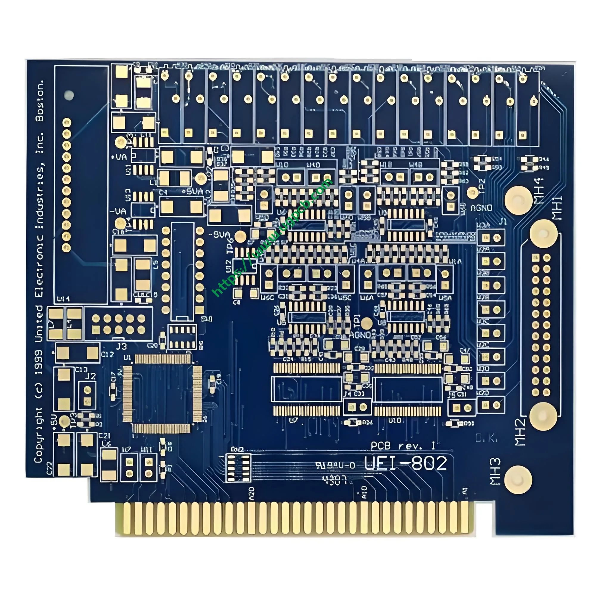
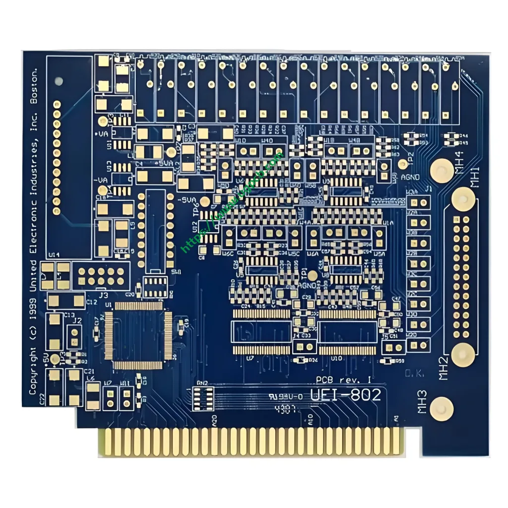
Um dedo de ouro de dupla face placa de circuito impresso (PCB) apresenta contatos folheados a ouro – comumente chamados de “dedos de ouro” – dispostos ao longo da borda da placa. Esses contatos criam um caminho elétrico conectável quando inseridos em um conector correspondente, como um slot ou soquete para cartão. Todos os sinais e energia fluem através desses terminais em formato de dedo.
O PCB de dedo dourado de dupla face da UGPCB usa um substrato FR4 com um design de 2 camadas. A espessura da placa é 1.6 milímetros, e ambas as camadas interna e externa têm 1 onças de cobre. O diâmetro mínimo da via perfurada é 0.3 milímetros, e a largura e o espaçamento do traço são ambos 0.15 milímetros. O acabamento da superfície é ouro de imersão (CONCORDAR) em todo o tabuleiro, com ouro duro galvanizado adicional aplicado seletivamente nas áreas dos dedos de ouro. Este produto oferece a flexibilidade de roteamento de uma placa dupla face juntamente com a confiabilidade comprovada das conexões Gold Finger. Ele atende a uma ampla variedade de sistemas eletrônicos que exigem interfaces de plug-in placa a placa.
2. Classificação e Posicionamento do Produto
De acordo com IPC-6012 (a rígida qualificação da placa impressa e especificação de desempenho), este produto se enquadra nas seguintes categorias:
| Dimensão de Classificação | Categoria |
|---|---|
| Por estrutura | PCB de dupla face – traços condutores em ambos os lados |
| Por Método de Interconexão | Com furos banhados (PTH) |
| Pela classe de desempenho IPC‑6012 | Aula 2 (produtos eletrônicos de serviço dedicado) – adequado para a maioria das aplicações de dedo de ouro |
| Por material de substrato | Laminado rígido FR4 (Grau S1141) |
| Por acabamento superficial | CONCORDAR (níquel sem eletrólito / ouro de imersão) + ouro duro galvanizado seletivo em dedos de ouro |
| Por função | PCB de dedo de ouro / PCB de conector de borda |
Este produto está posicionado como umconexão plug-in de média a alta confiabilidade solução. Ele combina a liberdade de design do roteamento de dupla face com a integridade do sinal dos conectores dourados.
3. Principais parâmetros técnicos
3.1 Substrato: FR4 + Laminado S1141
FR4 é o substrato rígido mais comum na indústria de PCB. Consiste em resina epóxi reforçada com fibra de vidro, que proporciona excelente resistência mecânica, isolamento elétrico, e resistência térmica. Este produto utiliza Laminado S1141 FR4 da Shengyi Tecnologia, que está em conformidade com IPC‑4101/21.
Principais indicadores de desempenho para S1141 (testado em 1.6 amostras mm) estão listados abaixo.
| Parâmetro | Valor típico | Método de teste |
|---|---|---|
| Temperatura de transição vítrea (Tg) | 140°C (DSC) | IPC‑TM‑650 2.4.25 |
| Temperatura de decomposição térmica (Td) | 310°C (5 % perda de peso) | IPC‑TM‑650 2.4.24.6 |
| CTE do eixo Z (antes de Tg) | 65 ppm/°C | IPC‑TM‑650 2.4.24 |
| CTE do eixo Z (depois de Tg) | 300 ppm/°C | IPC‑TM‑650 2.4.24 |
| Constante dielétrica (Dk, 1 MHz) | 4.6 | IPC‑TM‑650 2.5.5.9 |
| Fator de dissipação (Df, 1 MHz) | 0.015 | IPC‑TM‑650 2.5.5.9 |
| Classificação inflamabilidade | UL 94 V-0 | UL 94 |
| Absorção de Água | 0.15 % | IPC‑TM‑650 2.6.2.1 |
Fonte de dados: Folha de Dados Técnicos Shengyi S1141, compatível com IPC‑4101/21.
UL 94 V-0 é a classificação mais alta de retardante de chama na UL 94 teste de queima vertical. Requer que após duas aplicações de chama de 10 segundos, o tempo total de combustão em chamas para cada amostra não excede 10 segundos, e nenhuma gota flamejante acende o indicador de algodão. Isso garante que a PCB permaneça segura sob condições anormais de aquecimento ou curto-circuito.

3.2 Espessura da placa: 1.6 milímetros
O 1.6 mm de espessura é o padrão da indústria para PCBs rígidos. Também serve como espessura de linha de base para dados de propriedades de materiais S1141. Esta espessura atinge um equilíbrio ideal entre resistência mecânica, estabilidade de inserção, e custo de fabricação. É amplamente compatível com slots de conector padrão.
3.3 Espessura do Cobre: 1 onças (Aproximadamente 35 μm)
As folhas de cobre da camada interna e externa são1 onças (onça) , que é aproximadamente 35 μm de espessura. De acordo com IPC-6012, a espessura mínima de cobre acabado para Classe 1 e classe 2 placas é 48 μm. Começando com 1 a folha de onças garante que a espessura final após o processamento atenda a esses requisitos. Este peso de cobre suporta capacidade adequada de transporte de corrente (aproximadamente 4‑6 A, dependendo da largura do traço) preservando a precisão da gravação de linhas finas. A largura e o espaçamento do traço 0.15 milímetros (sobre 6 mil) são produzidos de forma confiável com 1 onças de cobre.
3.4 Diâmetro mínimo via: 0.3 milímetros
O diâmetro mínimo do furo mecânico perfurado é 0.3 milímetros, que está dentro da capacidade padrão da tecnologia de furo passante. Isto suporta furo passante revestido (PTH) processamento para garantir interconexão elétrica confiável entre camadas. Para IPC-6012, todos os PTHs devem passar no teste de estresse térmico (288 Mergulho de solda °C) para verificar a integridade estrutural.
3.5 Largura e espaçamento do traço: 0.15 milímetros / 0.15 milímetros
Uma largura de traço de 0.15 milímetros (aproximadamente 6 mil) e um espaçamento de 0.15 mm representam uma capacidade de linha fina na fabricação convencional de PCB. No 1 espessura de cobre de oz, um 0.15 O traço de mm pode transportar aproximadamente 0,5-0,8 A de corrente com base nos cálculos IPC-2221. Isso atende às necessidades da maioria das aplicações de transmissão de sinal e fonte de baixa potência. Esta combinação de largura e espaçamento garante confiabilidade, mantendo os custos de fabricação sob controle.
4. Acabamento superficial: Ouro de imersão mais dedos de ouro galvanizados
Este produto utiliza umprocesso combinado de acabamento superficial: ouro de imersão (CONCORDAR) em todo o tabuleiro, comouro duro galvanizado aplicado seletivamente nas áreas dos dedos dourados. Este é o processo padrão e ideal para PCBs Gold Finger.
4.1 Imersão Ouro (CONCORDAR) Processo
Níquel eletrolítico / Imersão Ouro (CONCORDAR) é um acabamento onde o níquel é primeiro depositado quimicamente na superfície do cobre, seguido por uma fina camada de ouro depositada através de uma reação de deslocamento.
PorIPC‑4552 Revisão A (publicado 2017) :
- Espessura do níquel: 3 μm para 6 μm (120 μin para 240 min)
- Espessura do ouro: 0.04 μm para 0.10 μm (1.6 μin para 4.0 min)
- Espessura de ouro recomendada: 0.04 μm para 0.07 μm (1.6 μin para 2.8 min)
Fonte de dados: IPC‑4552 – Especificação de desempenho para níquel eletrolítico / Imersão Ouro (CONCORDAR) Chapeamento para placas impressas.
Vantagens do ENIG:
- Superfície plana adequada para traços finos e pacotes BGA
- Excelente soldabilidade, suportando soldagem sem chumbo (por exemplo, SAC305)
- Forte resistência à oxidação com longa vida útil
- A fina camada de ouro mantém os custos gerenciáveis
4.2 Dedos de ouro galvanizados – a principal característica
As áreas dos dedos dourados recebemouro duro galvanizado adicional. Ao contrário do ouro macio usado no ENIG, ouro duro galvanizado contém endurecedores como cobalto ou níquel (liga de ouro-cobalto ou ouro-níquel). Sua dureza pode exceder HV 200, proporcionando uma resistência ao desgaste muito maior do que o ouro macio.
Por que os dedos de ouro devem usar ouro duro galvanizado?
O ouro ENIG é extremamente fino (apenas 0,04-0,10 μm) e macio (dureza abaixo de HV 90). Ele desaparece após apenas 3-5 ciclos de inserção. Ouro duro galvanizado, com uma espessura tipicamente acima 0.76 μm, pode suportar centenas ou até milhares de ciclos de inserção.
PorIPC‑4556 (Especificação de desempenho de ouro duro) :
| Classe de aplicação | Espessura Mínima de Ouro | Aplicações Típicas |
|---|---|---|
| Aula 2 (Durável) | ≥ 0.76 μm (30 min) | A maioria das aplicações de dedo de ouro |
| Aula 3 (Alta confiabilidade) | ≥ 1.27 μm (50 min) | Inserção de alto ciclo, industrial / militares |
| Camada inferior de níquel | 3-5 μm | Obrigatório para todos os depósitos de ouro duro |
Fonte de dados: IPC‑4556 – Especificação de desempenho para ouro duro galvanizado para conectores e dedos de ouro.
O processo de dedo de ouro galvanizado usado neste produto está em conformidade com a classe IPC‑4556 2 através da aula 3 padrões, garantindo vida útil de inserção e confiabilidade de contato.
5. Considerações de design
5.1 Chanframento de Dedo Dourado
A extremidade de inserção dos dedos de ouro deve serchanfrado para permitir uma entrada suave no slot do conector.
- Ângulo de chanfro: Normalmente 30° ou 45°
- Profundidade do chanfro: Para 1.6 espessura da placa mm, a profundidade do chanfro é normalmente 0,8-1,0 mm, deixando uma borda romba de 0,6-0,8 mm na ponta
- Espessura restante da ponta: Aproximadamente um terço a metade da espessura original da placa
- Requisito crítico: Nenhuma máscara de solda pode cobrir a área chanfrada, e a camada de ouro deve cobrir totalmente o chanfro chanfrado
5.2 Regras de design da área dos dedos dourados
- Os dedos dourados devem ser colocados na borda do tabuleiro em uma disposição ordenada
- O espaçamento mínimo entre dedos de ouro adjacentes deve ser ≥ 7 mil (aproximadamente 0.178 milímetros)
- A área do dedo de ouro deve ser claramente marcada nos arquivos Gerber com instruções explícitas de revestimento
5.3 Considerações sobre controle de impedância
O material FR4 tem uma constante dielétrica Dk = 4.6 no 1 MHz. Para 50 Ω single-ended ou 100 Ω controle de impedância diferencial, os designers podem ajustar a largura do traço e a espessura dielétrica. O 0.15 A largura e o espaçamento do traço em mm neste produto atendem à maioria dos requisitos de integridade de sinal para projetos padrão.
6. Princípio de funcionamento
Uma PCB de dedo de ouro dupla face opera por meio de dois mecanismos principais: contato elétrico etransmissão de sinal.
- Conexão elétrica: Os contatos dourados na borda da placa combinam fisicamente com os contatos de mola de metal dentro do slot do conector, estabelecendo um caminho elétrico de baixa resistência.
- Transmissão de sinal: O PCB rastreia sinais de rota de vários componentes (chips, resistores, capacitores, etc.) para os contatos de dedo dourado, que então transmite através do conector para a placa-mãe ou backplane. O design de dupla face permite roteamento em ambas as camadas superior e inferior, aumentando significativamente a densidade de roteamento e a flexibilidade de design.
- Plugabilidade: A camada de ouro duro galvanizado nos dedos de ouro fornece resistência ao desgaste suficiente para suportar vários ciclos de inserção sem degradar a resistência de contato ou a integridade do sinal.
7. Aplicativos e casos de uso
PCBs dedo de ouro de dupla face são amplamente utilizados em dispositivos eletrônicos que exigemconexões conectáveis. Aplicações comuns incluem:
| Área de Aplicação | Produtos Específicos |
|---|---|
| Computação & Servidores | Módulos de memória (DDR, DDR2, Ddr3, DDR4, DDR5), placas gráficas, placas de interface de rede, placas de expansão |
| Eletrônicos de consumo | Unidades USB, cartões de memória, leitores de cartão, smartphones, relógios inteligentes |
| Equipamento de comunicação | Roteadores, interruptores, módulos de comunicação |
| Controle industrial | Painéis de controle industriais, cartões de aquisição de dados, dispositivos de teste |
| Eletrônica Automotiva | Unidades de controle no veículo, sistemas de infoentretenimento |
| Dispositivos médicos | Módulos eletrônicos médicos (com suplemento médico IPC‑6012EM) |
| Aeroespacial | Módulos aviônicos (com suplemento aeroespacial IPC‑6012FS) |
PCBs de dedo dourado de dupla face FR4 são particularmente adequados paracomplexidade média, aplicações sensíveis ao custo que exigem conectividade plug-in.
8. Fluxo do Processo de Fabricação
UGPCB segue uma sequência de produção padrão para PCBs dedo de ouro de dupla face:
- Corte – Corte o laminado revestido de cobre FR4 nas dimensões do painel de trabalho.
- Perfuração - Furar 0.3 mm de furos passantes e furos de montagem.
- PTH / Chapeamento de painel – Aplicar deposição de cobre não eletrolítico em furos, então placa do painel.
- Transferência de padrão – Expor e desenvolver o padrão do circuito.
- Revestimento padrão – Circuitos e furos de placa eletrolítica para 1 onças de cobre.
- Gravura – Remova a folha de cobre desprotegida para formar os traços finais do circuito.
- Máscara de solda – Aplique tinta de máscara de solda verde ou de outra cor.
- Acabamento Superficial – ENIG – Aplicar níquel eletrolítico e ouro de imersão em toda a placa.
- Chapeamento de dedo de ouro – Galvanoplastia seletiva de ouro duro nas áreas dos dedos de ouro.
- Chanframento de Dedo Dourado – Chanfrar a extremidade de inserção.
- Teste Elétrico - Executar sonda voadora ou teste de fixação.
- Inspeção Visual – Inspecione conforme IPC‑A‑600.
- Embalagem & Envio – Embalagem a vácuo para proteção contra umidade.
9. Padrões de desempenho e qualidade
Este produto foi projetado e fabricado em estrita conformidade com os seguintes padrões internacionais:
| Padrão | Título | Escopo |
|---|---|---|
| IPC‑6012 | Especificação de qualificação e desempenho para placas impressas rígidas | Desempenho geral e confiabilidade |
| IPC-A-600 | Aceitabilidade de placas impressas | Aparência visual e critérios de aceitação |
| IPC‑4552 | Especificação de desempenho ENIG | Controle de processo de ouro por imersão |
| IPC‑4556 | Especificação de desempenho de ouro duro galvanizado | Processo de ouro duro de dedo de ouro |
| IPC‑4101/21 | Especificação para materiais de substrato de placa impressa rígida e multicamada | Especificações do material FR4 |
| UL 94 V-0 | Norma de Segurança – Inflamabilidade de Materiais Plásticos | Certificação retardante de chama |
10. Por que escolher UGPCB?
- Experiência profissional em fabricação de dedo de ouro – UGPCB possui capacidades maduras em galvanoplastia e chanframento.
- Controle de qualidade de ponta a ponta – Cada etapa, desde o corte até a inspeção final, é gerenciada de acordo com os padrões IPC.
- Materiais rastreáveis – Usa laminados FR4 de marca, como Shengyi S1141, com rastreabilidade clara da origem.
- Entrega rápida – Uma linha de produção dedicada de PCB de dupla face suporta prototipagem rápida e produção em volume.
- Suporte técnico – Fornece DFM (Design para fabricação) revisões e recomendações de controle de impedância.
11. Pergunte agora
A UGPCB está comprometida em fornecer soluções de PCB de dedo de ouro dupla face de alto valor para clientes em todo o mundo. Se você precisaprototipagem de amostra, produção experimental de pequenos lotes, ou fabricação em alto volume, temos a expertise para atender você.
Contate-nos para um orçamento:
- Forneça arquivos Gerber ou Projeto de PCB dados
- Especifique a espessura do revestimento de ouro (0.76 μm para 1.27 μm recomendado)
- Confirme o ângulo do chanfro (30° ou 45°) e quaisquer outros requisitos especiais
Declaração de fonte de dados
Os dados técnicos e referências padrão neste documento são provenientes de: Especificação de qualificação e desempenho IPC‑6012 para placas impressas rígidas; Especificação de desempenho IPC‑4552 para níquel eletrolítico / Imersão Ouro (CONCORDAR) Chapeamento para placas impressas; Especificação de desempenho IPC‑4556 para ouro duro galvanizado para conectores e dedos de ouro; Aceitabilidade IPC‑A‑600 de placas impressas; UL 94 Norma de Segurança – Inflamabilidade de Materiais Plásticos; e a Ficha Técnica Shengyi S1141 (compatível com IPC‑4101/21).













