

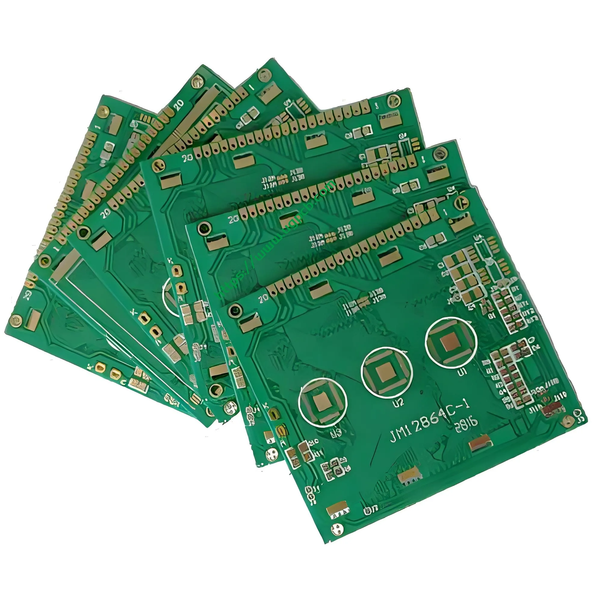
Visão geral do produto: Uma solução PCB de alta confiabilidade para condução de display LCD
UGPCB apresenta oPlaca de circuito PCB de tela de cristal líquido LCD (Modelo: UGPCB-LCD-001), um alto desempenho2-placa de circuito impresso FR-4 rígida de camada projetado especificamente para aplicações de acionamento de telas de cristal líquido. Este produto usa laminado revestido de cobre de alta qualidade Kingboard KB6165F como material de base, com uma espessura de placa de 1.6 milímetros e 1 onça de folha de cobre (aproximadamente 35 μm). O acabamento superficial empregaCONCORDAR (Níquel eletrolítico/ouro de imersão) processo em 2U” . A diretoria mede 147.2 × 65 milímetros, com um diâmetro mínimo de furo de 0.22 mm e largura/espaçamento mínimo de linha de 0.3 mm/0,27 mm.
EssePWB da exposição do LCD serve como portador de circuito crítico que conecta chips de driver de vídeo a painéis de vidro de cristal líquido. Ele encontra amplas aplicações em módulos de display LCD de pequeno e médio porte, displays de painel de controle industrial, displays de sistema de infoentretenimento automotivo, e interfaces de interação homem-máquina domésticas inteligentes.
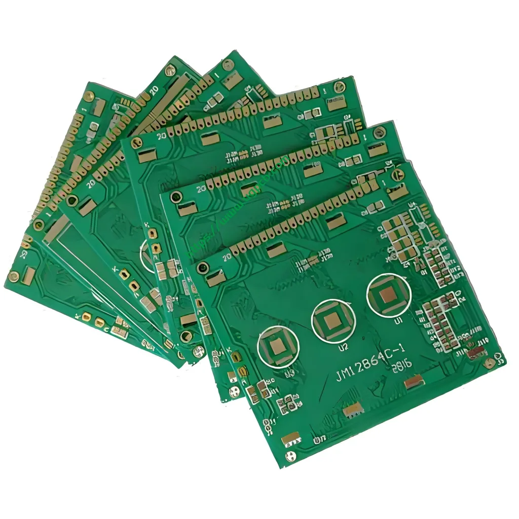
Definição do Produto: O que é uma PCB com tela de cristal líquido LCD?
Um PCB de tela de cristal líquido LCD (Placa de circuito impresso) é uma placa de circuito especializada projetada para sistemas de acionamento de telas de cristal líquido. Ele executa três funções principais: transmissão de sinal de condução, distribuição de energia, e roteamento de sinal de controle de tempo. Ao contrário do padrão Placas de circuito PCB, um PWB da exposição do LCD exige tolerâncias mais rígidas na precisão da largura da linha, controle de impedância, e planicidade da superfície.
Este produto pertence aoPCB rígido de dupla face categoria com 2 camadas (2eu). Ele usa material retardador de chama de grau FR-4 (UL 94 V-0 Avaliado) e suporta SMT (Tecnologia de montagem em superfície) e processos de montagem híbrida de componentes através do furo. A placa atende à classe IPC-6012 2 requisitos de desempenho, tornando-o adequado para aplicações em eletrônica industrial e eletrônica de consumo.
Especificações de projeto: Parâmetros críticos para engenharia de PCB LCD
Material de substrato: A vantagem do KB6165F
Este produto usa laminado revestido de cobre Kingboard KB6165F, que oferece as seguintes características principais de desempenho:
- Temperatura de transição vítrea (Tg): ≥150°C, garantindo estabilidade dimensional durante processos de soldagem por refluxo sem chumbo
- Temperatura de decomposição térmica (Td): 325°C, proporcionando excelente confiabilidade térmica
- Classificação inflamabilidade: UL 94 V-0, com chama autoextinguível dentro 10 segundos em testes de queima vertical
- CTE (Coeficiente de Expansão Térmica): 12–15 ppm/°C na direção X-Y, 40–230 ppm/°C na direção Z, oferecendo boa correspondência térmica com ICs de driver de LCD
- CAF (Filamento Anódico Condutivo) Resistência: Excelente desempenho anti-CAF garantindo confiabilidade a longo prazo
- Compatível sem chumbo: Atende aos requisitos ambientais RoHS
De acordo com os padrões de design IPC-2221, materiais com Tg ≥150°C são adequados para processos de montagem sem chumbo, capaz de manter a integridade estrutural sob temperaturas de pico de soldagem por refluxo atingindo 245–260°C.
Contagem de camadas e design de empilhamento
As características do produto 2 camadas (2eu) com um padrão 1.6 espessura da placa mm. Para IPC-2221, 1.6 mm representa a especificação de espessura mais comumente usada para PCB, equilibrando resistência mecânica com conveniência de montagem.
Largura de linha e design de espaçamento
A largura mínima da linha de 0.3 mm e espaçamento mínimo entre linhas de 0.27 mm são parâmetros cuidadosamente selecionados paraPlaca de circuito impresso do driver LCD integridade do sinal. Sob os padrões IPC-2221, o requisito de espaçamento mínimo para tensão convencional (≤30V) traços de sinal digital são 0.1 milímetros (4 mil). Este produto 0.27 milímetros (aproximadamente 10.6 mil) o espaçamento excede em muito o requisito mínimo do IPC, fornecendo ampla margem para qualidade do sinal.
Referência de cálculo de projeto (com base na fórmula simplificada da capacidade de transporte de corrente do condutor da camada externa IPC-2221):
Capacidade de transporte de corrente de rastreamento da camada externa ≈ k × ΔT ^ 0,448 × W ^ 0,725 × T ^ 0,725
Onde k = 0.048 (para camada externa). Com um aumento de temperatura de 10°C, um 0.3 traço mm com 1 onças de espessura de cobre fornecem uma capacidade teórica de transporte de corrente de aproximadamente 1,2–1,5 A – suficiente para os requisitos de energia e rastreamento de sinal de placas de driver LCD convencionais.
Diâmetro mínimo do furo
O diâmetro mínimo do furo de 0.22 milímetros (aproximadamente 8.7 mil) se enquadra na categoria de perfuração de precisão. Sob IPC-6012, a tolerância padrão do diâmetro do furo perfurado é de ±0,08 mm (aproximadamente ±3 mil) . Para 0.22 mm microvias, as tolerâncias de fabricação são normalmente controladas dentro de ±0,05 mm.
Acabamento superficial: CONCORDO que 2U”
OCONCORDAR (Níquel eletrolítico/ouro de imersão) acabamento superficial com 2U” espessura do ouro (aproximadamente 0.05 μm) está em conformidade com os requisitos IPC-4552. IPC-4552 Revisão A (emitido em 2017) especifica a espessura do depósito de ouro de 0.04 μm para 0.10 μm (1.6 μin para 4.0 min) e espessura de níquel de 3 μm para 6 μm.
Vantagens do acabamento superficial ENIG:
- Excelente soldabilidade suportando múltiplos ciclos de refluxo
- Forte capacidade de ligação de fios
- Resistência superior à oxidação e à corrosão
- Superfície plana adequada para montagem de componentes de passo fino
- Vida útil prolongada
Princípio Operacional: Mecanismos de transmissão de sinal da PCB do display LCD
OPCB de tela de cristal líquido LCD opera em duas funções principais: transmissão de sinal edistribuição de energia.
1. Transmissão de sinal do driver de exibição: Exibir dados do chip controlador principal (MCU/SoC) viaja peloPlaca de circuito PCB via microstrip ou traços de stripline para o IC do driver LCD. O driver IC converte sinais digitais em tensões analógicas em escala de cinza, que são então emitidos através doPCBtraços finos dos eletrodos ITO no painel de vidro de cristal líquido, controlando o ângulo de torção das moléculas de cristal líquido para produzir a imagem exibida.
2. Roteamento de sinal de controle de tempo: OPWB da exposição do LCD carrega sinais de temporização críticos, incluindo VSYNC (Sincronização vertical), HSYNC (Sincronização horizontal), DCLK (Relógio de pixels), e DE (Habilitação de dados). O atraso de transmissão e a correspondência de impedância desses sinais afetam diretamente a qualidade da exibição.
3. Distribuição de gerenciamento de energia: OPlaca de circuito LCD converte a potência de entrada (tipicamente 3.3 V ou 5 V) através de circuitos de conversão DC-DC para gerar os múltiplos níveis de tensão exigidos pelo painel LCD, incluindo VGH (tensão de porta, tipicamente +15 V para +30 V), Cf. (tensão de desligamento, normalmente −5 V a −15 V), e AVDD (tensão de alimentação analógica).
Classificação do Produto: Categorias de PCB LCD
PCBs de tela de cristal líquido LCD pode ser classificado nas seguintes dimensões:
Por contagem de camadas
- Placas unilaterais: Usado para displays LCD de código de segmento simples
- Placas dupla-face (2eu): A categoria deste produto, usado para drivers de display TFT-LCD de pequeno a médio porte
- Placas multicamadas (4L e acima): Usado para alta resolução, módulos de exibição de grande formato
Por acabamento superficial
- Placas ENIG: A categoria deste produto, oferecendo o melhor desempenho geral
- Placas OSP: Menor custo, adequado para produtos eletrônicos de consumo de ciclo de vida curto
- Placas HASL: Adequado para placas de driver LCD com pinos mais largos
Por aplicação
- PCBs LCD de eletrônicos de consumo: Monitores secundários de smartphones, monitores de smartwatch, telas de e-reader
- PCBs LCD de controle industrial: IHM industrial, exibições do painel de instrumentos, Drivers de exibição do painel de operação CNC
- PCBs LCD automotivos: Sistemas de infoentretenimento no veículo, grupos de instrumentos digitais, Placas de controle de exibição HUD
- PCBs de LCD para dispositivos médicos: Monitores de pacientes, equipamento de diagnóstico por ultrassom, placas de driver de exibição do sistema de imagens médicas
Especificações principais de desempenho
| Parâmetro | Especificação | Padrão de Referência |
|---|---|---|
| Material laminado | KB6165F (Kingboard) | - |
| Tipo laminado | Laminado revestido de cobre com tecido de vidro FR-4 | UL 94 V-0 |
| Contagem de camadas | 2 camadas (2eu) | - |
| Espessura da placa | 1.6 milímetros | IPC-2221 |
| Espessura de cobre da camada externa | 1 onças (35 μm) | IPC-6012 Classe 2 |
| Acabamento superficial | APENAS 2U” (0.05 μm Au) | IPC-4552 |
| Espessura da camada de níquel | 3–6 μm (camada inferior) | IPC-4552 Rev A |
| Diâmetro mínimo do furo | 0.22 milímetros | IPC-6012 |
| Largura mínima da linha | 0.3 milímetros | IPC-2221 |
| Espaçamento mínimo entre linhas | 0.27 milímetros | IPC-2221 |
| Dimensões da placa | 147.2 × 65 milímetros | - |
| Tg (Temperatura de transição vítrea) | ≥150°C | - |
| Td (Temperatura de decomposição térmica) | 325°C | - |
| CTE (Direção XY) | 12–15 ppm/°C | - |
| Classificação inflamabilidade | UL 94 V-0 | UL 94 |
| Resistência ao arco | ≥60 segundos | - |
| Resistividade da superfície | ≥2,6 × 10⁸ MΩ | - |
| Resistividade de volume | ≥3,4 × 10⁹ MΩ·cm | - |
Análise da Estrutura do Produto
OPCB de tela de cristal líquido LCD estrutura compreende as seguintes camadas de fora para dentro:
1. Camada Externa – Acabamento Superficial ENIG: Camada de ouro em 2U” (aproximadamente 0.05 μm) protege a camada subjacente de níquel da oxidação. A camada inferior de níquel de 3–6 μm serve como uma barreira de difusão entre o cobre e o ouro.
2. Camada de folha de cobre: 1 onças (aproximadamente 35 μm) folha de cobre eletrodepositada, gravado para formar o padrão de circuito.
3. Camada Dielétrica: Tecido de vidro grau FR-4 impregnado com resina epóxi, aproximadamente 0.7 mm de espessura (camada única), fornecendo isolamento elétrico e suporte mecânico.
4. Camada de folha de cobre: Camada inferior 1 onças de cobre formando o padrão do circuito inferior.
5. Camada Externa – Acabamento Superficial ENIG: Tratamento ENIG simétrico combinando com a camada superior.
Recursos do produto: Por que escolher o display LCD da UGPCB?
① Fabricação de alta precisão: Diâmetro mínimo do furo de 0.22 mm e largura/espaçamento mínimo de linha de 0.3 mm/0,27 mm suportam os requisitos de roteamento de placas de driver LCD de alta densidade.
② Materiais de substrato premium: Kingboard KB6165F material FR-4 de alta qualidade com Tg ≥150°C e UL 94 V-0 a classificação de inflamabilidade garante compatibilidade de processo sem chumbo e confiabilidade a longo prazo.
③ Acabamento de superfície padronizado: APENAS 2U” processo está em conformidade com IPC-4552, proporcionando excelente soldabilidade, resistência à oxidação, e vida útil prolongada.
④ Rigoroso controle de qualidade: Os produtos passam por controle de qualidade de processo completo de acordo com a classe IPC-6012 2 padrões, tolerância do diâmetro do furo de cobertura (±0,08mm), espessura do cobre do furo (≥20 μm), integridade da máscara de solda, e testes elétricos.
⑤ Design otimizado para LCD: Controle de impedância, integridade do sinal, e a integridade da energia são otimizadas especificamente para aplicações de acionamento de telas de cristal líquido.
Processo de fabricação: Da matéria-prima ao produto acabado
UGPCB segue um rigoroso processo de fabricação padrão paraPCBs de display LCD:
1. Corte de materiais →2. Transferência de padrão de camada interna (posicionamento da broca e marcas de registro) →3. Perfuração (diâmetro mínimo do furo 0.22 milímetros ± 0.08 milímetros) →4. Deposição/galvanoplastia de cobre não eletrolítico (metalização de furo, espessura do cobre do furo ≥20 μm) →5. Transferência de padrão de camada externa (Largura da linha 0.3 milímetros / espaçamento 0.27 milímetros) →6. Revestimento padrão (acúmulo de cobre para 1 onças) →7. Gravura →8. Impressão de máscara de solda →9. Acabamento de Superfície ENIG (CONCORDAR, espessura de ouro 2U”) →10. Perfil (dimensões 147.2 × 65 milímetros) →11. Teste elétrico (100% teste elétrico) →12. Inspeção Final (AOI + inspeção visual) →13. Embalagem e Envio
Cenários de aplicação típicos
📱 Eletrônicos de consumo: Monitores secundários de smartphones, monitores de smartwatch, PCBs de driver de tela de leitor eletrônico.
🏭 Controle Industrial: Interfaces homem-máquina PLC (IHM), displays de instrumentos industriais, Placas de driver de exibição do painel de operação CNC.
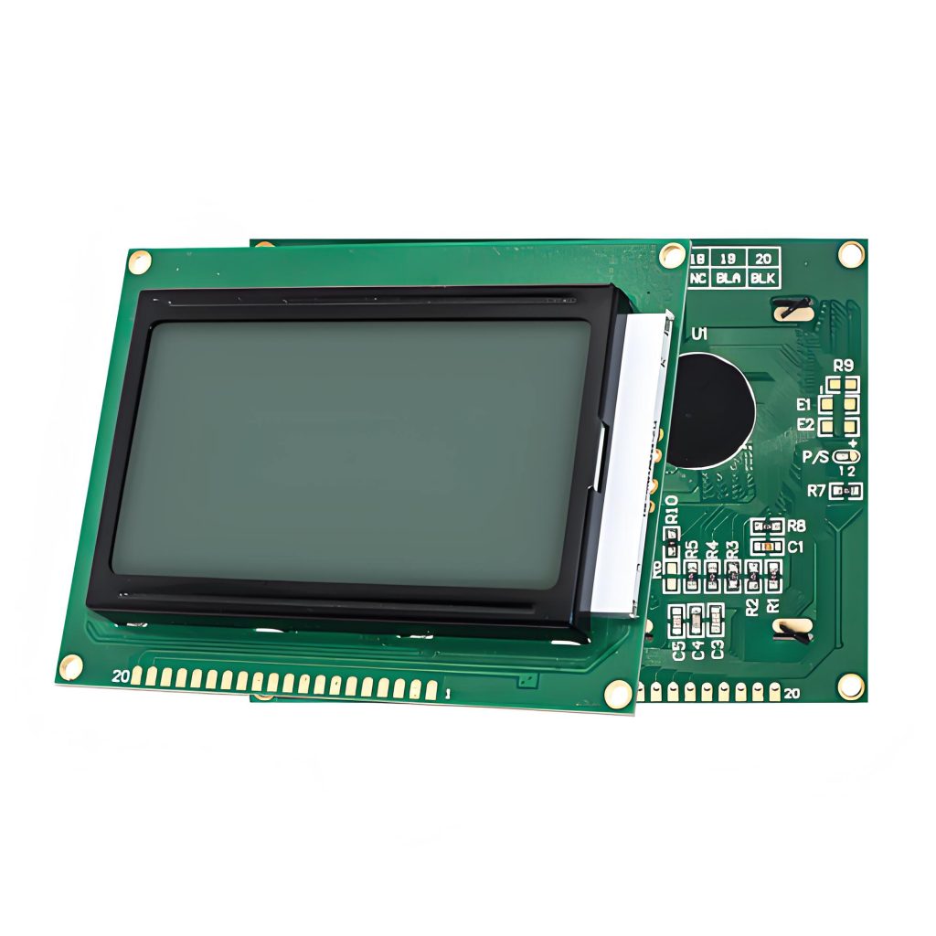
🚗 Eletrônica Automotiva: Sistemas de infoentretenimento no veículo, grupos de instrumentos digitais, exibição frontal (HUD) exibir PCBs de controle.
🏥 Dispositivos Médicos: Monitores de pacientes, equipamento de diagnóstico por ultrassom, placas de circuito do driver de exibição do sistema de imagens médicas.
🏠 Casa Inteligente: Exibições do sistema de controle de acesso inteligente, painéis de controle de aparelhos inteligentes, construção de PCBs de módulo de exibição de sistema de intercomunicação.
Por que escolher UGPCB?
UGPCB traz anos de PWB da exposição do LCD experiência de fabricação para cada projeto. Usamos matérias-primas premium como Kingboard KB6165F, aplicar estritamente a classe IPC-6012 2 padrões de qualidade, e operar equipamentos de perfuração e padronização de circuitos de alta precisão. Se você precisa LCD Prototipagem de PCB ou produção em volume, UGPCB oferece alta precisão, soluções de produtos de alta confiabilidade.
📞 Obtenha sua solução de PCB com display LCD hoje mesmo
UGPCB's PCBs de tela de cristal líquido LCD foram implantados com sucesso em inúmeras indústrias, automotivo, e projetos de exibição de eletrônicos de consumo. Se você precisa Prototipagem de PCB LCD para validação de projeto ou PCBA serviços de montagem chave na mão, UGPCB fornece suporte completo ao processo, desde a fabricação de PCB até PCBA Montagem SMT.
Entre em contato com a equipe profissional da UGPCB hoje para obter sua solução personalizada de PCB com display LCD!
📧 E-mail: [info@ugpcb.com]
📞 Telefone: [+86-755-XXXXXXXX]
🌐 Site: [www.ugpcb.com]
Atribuição de fonte de dados
Os padrões técnicos e dados citados neste documento são derivados das seguintes fontes autorizadas:
- IPC-6012 -Especificação de qualificação e desempenho para placas impressas rígidas – Define tolerâncias de diâmetro de furo de PCB (padrão ±0,08 mm), espessura do cobre do furo (Aula 2 ≥20 μm), e requisitos de classe de desempenho
- IPC-2221 -Padrão genérico para design de placas impressas – Especifica requisitos de projeto de largura/espaçamento de linha e fórmulas de cálculo de capacidade de transporte de corrente
- IPC-4552 Revisão A (publicado 2017) -Especificação de desempenho para níquel eletrolítico/ouro de imersão (CONCORDAR) Chapeamento para placas impressas – Especifica os requisitos de espessura do depósito ENIG: níquel 3–6 μm, ouro 0,04–0,10 μm
- UL 94 -Norma para Segurança de Inflamabilidade de Materiais Plásticos para Peças em Dispositivos e Eletrodomésticos –V-0 classificação requer autoextinção de chama dentro 10 segundos
- Folha de dados do produto Kingboard KB6165F – Parâmetros técnicos do substrato (Tg ≥150°C, Td 325°C, UL 94 V-0, etc.)
- GB/T 4677 -Métodos de teste para placas impressas – Usado em conjunto com padrões IPC como referências de inspeção













