

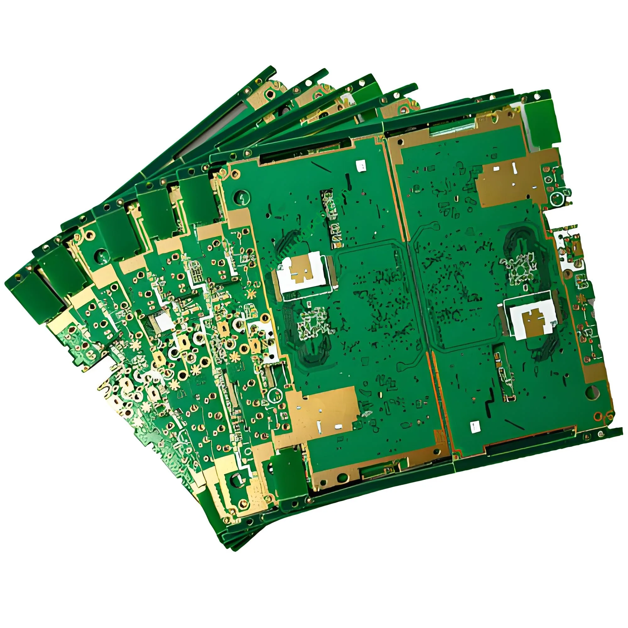
EU. Visão geral do produto: Uma placa PCB projetada para sistemas de campainha sem fio
A placa de circuito PCB da campainha sem fio é um componente eletrônico essencial em sistemas domésticos e de segurança inteligentes. UGPCB oferece esta placa construída com laminado revestido de cobre de alto desempenho Kingboard KB6165F. O processo de fabricação segue rígidos controles de qualidade.
Esta PCB de campainha sem fio é uma placa dupla-face de 2 camadas placa de circuito impresso. Tem espessura de 1,0mm e medidas 79.48 × 35,6 mm. Essas dimensões se encaixam perfeitamente em gabinetes compactos de campainha sem fio. A placa usa um HASL sem chumbo (Nivelamento de solda com ar quente) acabamento superficial. Este acabamento atende aos requisitos ambientais da RoHS, ao mesmo tempo que oferece excelente soldabilidade.
Campainhas sem fio servem como primeira linha de defesa na segurança doméstica. A confiabilidade de suas placas de circuito determina diretamente a vida útil do produto e a experiência do usuário. UGPCB entende este requisito crítico. Selecionamos cuidadosamente os materiais e controlamos cada etapa do processo para fornecer campainha sem fio de alta qualidade Placas PCB para clientes em todo o mundo.
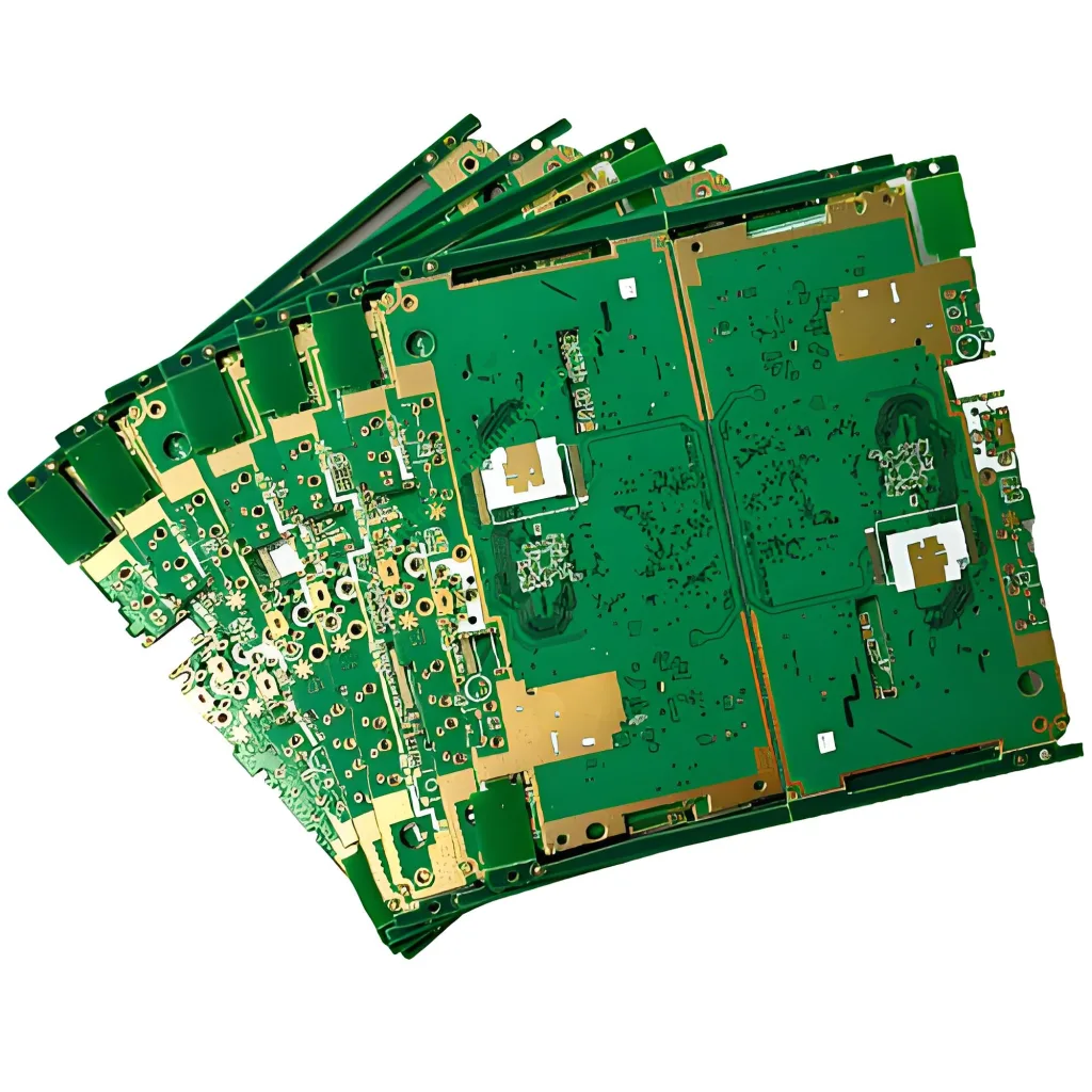
II. Definição de produto e posicionamento na indústria
UMplaca de circuito PCB de campainha sem fio é uma placa de circuito impresso usada em sistemas de campainha sem fio. Geralmente consiste em duas partes: uma placa transmissora e uma placa receptora. A PCB do transmissor carrega o chip codificador (como HT12E), um módulo transmissor sem fio de 433 MHz, e o circuito do interruptor de botão. O PCB receptor carrega o chip decodificador (como HT12D), o módulo receptor sem fio, o amplificador de áudio, e o circuito do driver do alto-falante.
Do ponto de vista da classificação de PCB, este produto é umplaca de circuito impresso dupla face rígida (PCB rígido de dupla face) . Pode ser ainda classificado da seguinte forma:
| Dimensão de Classificação | Categoria |
|---|---|
| Camadas condutivas | Frente e verso (2eu) |
| Rigidez do Substrato | Placa Rígida |
| Acabamento superficial | HASL sem chumbo |
| Classificação inflamabilidade | UL 94 V-0 |
| Classe de desempenho IPC | Aula 2 (Produtos eletrônicos de serviço dedicado) |
Este produto está em conformidade com IPC-6012Especificação de qualificação e desempenho para placas impressas rígidas. Seu material de substrato, KB6165F, atende aos requisitos da especificação IPC-4101/99.
III. Principais parâmetros técnicos
3.1 Material de substrato: Laminado revestido de cobre Kingboard KB6165F
KB6165F é umlaminado revestido de cobre com tecido de vidro Tg150 sem chumbo fabricado por Kingboard Laminates Holdings Limited. Pertence à família de laminados de tecido de vidro epóxi grau FR-4. Os principais indicadores de desempenho são os seguintes:
- Temperatura de transição vítrea (Tg) : 154°C (Método de teste: IPC-TM-650 2.4.25)
- Zis Z CTE (Coeficiente de Expansão Térmica) : 40 ppm/°C (50–260ºC), expansão total 3.1% (Método de teste: IPC-TM-650 2.4.24)
- Tempo de delaminação T-288 : >30 minutos (Método de teste: IPC-TM-650 2.4.24.1)
- Temperatura de decomposição térmica (Td, 5% perda de peso) : 346°C (Método de teste: IPC-TM-650 2.4.24.6)
- Classificação inflamabilidade : UL 94 V-0
- Constante dielétrica (Dk) @ 1 GHz : 4.6 (Método de teste: IPC-TM-650 2.5.5.2)
- Fator de dissipação (Df) @ 1 GHz : 0.016 (Método de teste: IPC-TM-650 2.5.5.2)
- Força de casca (1 onça de folha de cobre) : 1.4 N/mm (Método de teste: IPC-TM-650 2.4.8)
- Força de flexão : 550 N/mm² (longitudinal) / 485 N/mm² (transversal) (Método de teste: IPC-TM-650 2.4.4)
- Absorção de umidade : 0.10% (Método de teste: IPC-TM-650 2.6.2.1)
- Estresse térmico : ≥240 segundos (Método de teste: IPC-TM-650 2.4.13.1)
Uma alta Tg (>150°C) significa que este substrato pode suportar as altas temperaturas dos processos de soldagem sem chumbo. Previne eficazmente o empenamento e a delaminação da placa durante a montagem. É excelente anti-CAF (Filamento Anódico Condutivo) o desempenho garante confiabilidade em ambientes úmidos e sob condições de ligação prolongada.
3.2 Espessura da placa e contagem de camadas
A espessura da placa é1.0milímetros com2 camadas (2eu) . Esta espessura fornece resistência mecânica suficiente, ao mesmo tempo que atende aos requisitos de design fino e compacto de produtos de campainha sem fio. O design de camada dupla permite o layout adequado dos circuitos de RF, circuitos de energia, e circuitos de controle nas placas do transmissor e do receptor. Isso otimiza a integridade do sinal e a integridade da energia.
3.3 Dimensões
As dimensões são79.48mm × 35,6 mm. Este tamanho compacto é otimizado para o espaço interno de produtos de campainha sem fio. Ele acomoda todos os circuitos funcionais enquanto cabe facilmente em vários gabinetes de campainha.
3.4 Abertura Mínima
A abertura mínima é0.332milímetros. De acordo com os requisitos IPC-6012 para furos revestidos, este tamanho de abertura atende às necessidades de confiabilidade da inserção de cabos de componentes e via metalização em placas PCB de campainha sem fio.
3.5 Largura e espaçamento do traço
A largura do traço é0.42milímetros e o espaçamento entre traços é0.46milímetros. De acordo com IPC-2221Padrão genérico para design de placas impressas, a capacidade de transporte de corrente pode ser calculada usando a seguinte fórmula:
Onde:
- = Capacidade máxima de transporte de corrente (amperes)
- = Fator de correção (0.048 para camadas externas, 0.024 para camadas internas)
- = Aumento de temperatura permitido (°C)
- = Área da seção transversal do condutor (milésimos quadrados)
Para traços de camada externa com 1 onça de folha de cobre (1.37 milímetros de espessura) e uma largura de traço de 0,42 mm (aproximadamente 16.5 milésimos), a área da seção transversal é:
Com um aumento de temperatura de 10°C, a capacidade teórica de transporte de corrente é:
Esta capacidade de corrente atende totalmente aos requisitos de circuitos de RF de baixa potência e circuitos de controle digital em placas PCB de campainha sem fio.
3.6 Espessura da folha de cobre
A espessura da folha de cobre é1/1OZ (1 onças em ambas as camadas externas, aproximadamente 35μm). Esta espessura proporciona um excelente equilíbrio entre a capacidade de transporte de corrente, condutividade térmica, e custo. É a configuração padrão para PCBs de eletrônicos de consumo.
3.7 Acabamento superficial: HASL sem chumbo
O acabamento superficial éHASL sem chumbo (Nivelamento de solda com ar quente) . Neste processo, o PCB está imerso em liga de solda fundida sem chumbo (normalmente Sn99.3Cu0.6). Facas de ar quente de alta pressão sopram pela superfície para remover o excesso de solda.
As principais vantagens do acabamento superficial HASL sem chumbo incluem:
- Excelente soldabilidade : Adequado para vários ciclos de soldagem
- Longa vida útil : A liga de solda proporciona boa estabilidade de armazenamento
- Custo-benefício : Mais económico que ENIG e outros acabamentos
- Conformidade com RoHS : Não contém chumbo ou outras substâncias restritas
Este acabamento superficial atende aos requisitos de revestimento especificados em IPC-6012.
3.8 Máscara de solda e legenda
A máscara de solda étinta verde e a lenda étinta branca. A máscara de solda verde é a escolha mais popular na indústria de PCB. Oferece excelentes propriedades de isolamento, resistência ao calor, e clareza visual. A legenda branca garante que os designadores dos componentes, marcas de polaridade, e outras informações permanecem claramente legíveis.
4. Diretrizes de Design e Princípios Operacionais
4.1 Diretrizes de projeto
Campainha sem fio Projeto de PCB requer atenção a diversas áreas críticas:
(1) Projeto de circuito RF
Campainhas sem fio normalmente operam na banda ISM de 433 MHz. Os traços de RF devem ser projetados como linhas microstrip de impedância característica de 50Ω ou guias de onda coplanares. A largura do traço deve ser calculada com precisão com base na Material da PCB parâmetros (Dk = 4.6). A antena deve ser colocada perto da borda do PCB. Evite colocá-lo no meio do tabuleiro ou cercá-lo com grandes planos de terra.
(2) Integridade de energia
Os circuitos de gerenciamento de energia nas placas do transmissor e do receptor exigem um layout adequado. Coloque os capacitores de desacoplamento próximos aos pinos do IC seguindo as “próximo e múltiplo” princípio.
(3) Mitigação de interferência
Coloque o circuito receptor em um canto da PCB, longe de fontes de alimentação e outras fontes de ruído. O circuito oscilador de cristal precisa de seu próprio plano de aterramento e deve ser colocado o mais próximo possível do MCU.
(4) Gerenciamento térmico
A espessura da placa de 1,0 mm combinada com 1 a folha de cobre de onças fornece boa condutividade térmica. Isso dissipa efetivamente o calor dos amplificadores de potência de RF e outros componentes geradores de calor.
4.2 Princípios Operacionais
Um sistema de campainha sem fio consiste em um transmissor e um receptor:
Operação do Transmissor : Quando um usuário pressiona o botão da campainha, o chip codificador (como HT12E) na PCB do transmissor codifica o sinal do botão. O módulo transmissor RF de 433 MHz envia então este sinal codificado sem fio. O transmissor normalmente consome cerca de 5,6 mA durante a operação.
Operação do receptor : O módulo receptor RF de 433 MHz na PCB do receptor monitora continuamente os sinais sem fio. Quando recebe um sinal codificado correspondente, o chip decodificador (como HT12D) decodifica. Isso aciona o circuito do amplificador de áudio para acionar o alto-falante e produzir o toque da campainha.
V. Recursos do produto e vantagens de desempenho
5.1 Recursos do produto
| Recurso | Descrição |
|---|---|
| Substrato de alta confiabilidade | Laminado Kingboard KB6165F Tg150, UL 94 V-0 retardador de chama |
| Processo sem chumbo ecologicamente correto | Acabamento de superfície HASL sem chumbo, Compatível com RoHS |
| Capacidade de fabricação de precisão | Abertura mínima 0,332 mm, suporta roteamento de alta densidade |
| Excelente resistência ao calor | T-288 >30min, resiste a temperaturas de soldagem por refluxo sem chumbo |
| Desempenho elétrico superior | Dk = 4,6, Df = 0,016 a 1 GHz, adequado para aplicações de RF |
| Alta precisão dimensional | Dimensões precisas de 79,48 × 35,6 mm, cabe em caixas de campainha padrão |
5.2 Vantagens de desempenho
(1) Conformidade com padrões internacionais
O produto foi projetado e fabricado em conformidade com IPC-6012Especificação de qualificação e desempenho para placas impressas rígidas e IPC-A-600Aceitabilidade de placas impressas. O substrato atende aos requisitos da especificação IPC-4101/99.
(2) Certificação de segurança da UL
O substrato KB6165F obteve certificação UL (Arquivo UL não. E123995). Sua classificação de retardamento de chama atende à UL 94 V-0. Também está em conformidade com UL 796Padrão para placas de fiação impressa para placas rígidas usadas como componentes em dispositivos ou aparelhos.
(3) Robustez Ambiental
O CTE do eixo Z baixo (40 ppm/°C) e excelente desempenho anti-CAF garantem confiabilidade a longo prazo sob ciclos de temperatura e condições úmidas.
VI. Fluxo do Processo de Fabricação
UGPCB segue um processo de fabricação padronizado para placas PCB de campainha sem fio:
① Inspeção de materiais recebidos → Inspecione o substrato e a folha de cobre de acordo com IPC-A-600
② Formação do Circuito da Camada Interna → Filme seco laminado, expor, desenvolver, e gravar para formar padrões de circuito de camada interna
③ Laminação → Núcleos da camada interna laminada com pré-impregnado (Pp) sob alta temperatura e pressão
④ Perfuração → CNC perfuração, abertura mínima 0,332 mm
⑤ Deposição de cobre sem eletricidade / Chapeamento de painel → Deposição de cobre não eletrolítico + galvanoplastia de placa completa para conexão elétrica intercalar
⑥ Formação do Circuito da Camada Externa → Filme laminado, expor, desenvolver, placa padrão, e gravar para formar circuitos de camada externa
⑦ Aplicação de máscara de solda → Aplique tinta verde para máscara de solda para proteger os circuitos e evitar curtos-circuitos de solda
⑧ Acabamento de superfície → HASL sem chumbo (Nivelamento de solda com ar quente)
⑨ Impressão de legenda → Imprimir legenda branca para identificar designadores de componentes
⑩ Roteamento → Roteamento ou puncionamento CNC para dimensões finais de 79,48 × 35,6 mm
⑪ Teste Elétrico → Sonda voadora ou teste de fixação para 100% detecção aberta/curta
⑫ Inspeção Final → Inspeção visual e dimensional conforme IPC-A-600
⑬ Embalagem e envio → Embalagem a vácuo com proteção contra umidade
VII. Cenários de aplicativos e mercados de uso final
As placas PCB de campainha sem fio são amplamente utilizadas nas seguintes aplicações:
| Cenário de aplicação | Descrição |
|---|---|
| Campainhas sem fio residenciais | Sistemas de campainha de entrada residencial com transmissor externo e receptor interno |
| Intercomunicadores para edifícios inteligentes | Unidades de chamada sem fio para sistemas de acesso a prédios de apartamentos |
| Sistemas de chamada de serviço hoteleiro | Módulos transmissores sem fio para botões de chamada de serviço de quarto de hotel |
| Sistemas de chamada de emergência para atendimento a idosos | PCBs transmissores sem fio para botões de ajuda de emergência para idosos |
| Dispositivos IoT domésticos inteligentes | Campainhas inteligentes com módulos Wi-Fi integrados |
| Sistemas de Segurança e Vigilância | Unidades de disparo e alarme sem fio para equipamentos de segurança |
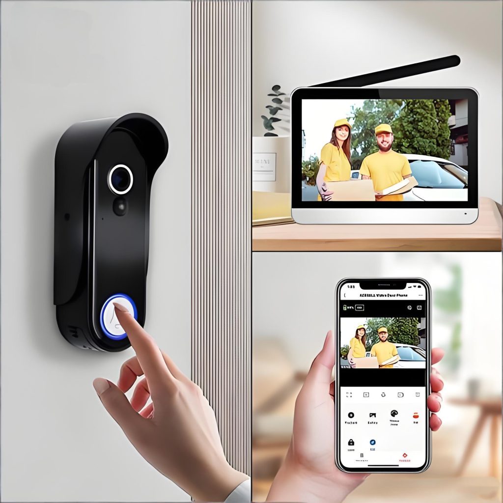
Placas PCB de campainha sem fio são componentes essenciais em eletrônicos de consumo e dispositivos domésticos inteligentes. A demanda do mercado continua a crescer. À medida que a adoção de casas inteligentes acelera, a necessidade de alta qualidade, placas PCB de campainha sem fio de alta confiabilidade estão aumentando rapidamente.
VIII. Por que escolher placas PCB de campainha sem fio UGPCB?
✅ Material de substrato premium : Laminado Kingboard KB6165F Tg150 com UL 94 V-0 o retardamento de chama garante segurança e confiabilidade do produto
✅ Conformidade com padrões internacionais : Projeto e fabricação estão em conformidade com IPC-6012, IPC-A-600, IPC-2221, e outras especificações internacionais
✅ Processo sem chumbo ecologicamente correto : O acabamento superficial HASL sem chumbo atende aos requisitos ambientais RoHS
✅ Capacidade de fabricação de precisão : Abertura mínima 0,332 mm, largura/espaçamento do traço 0,42/0,46 mm para necessidades de roteamento de alta precisão
✅ Suporte profissional de design de RF : 50Controle de impedância Ω e outro suporte de design profissional para aplicações de campainha sem fio de 433 MHz
✅ Entrega rápida : Protótipos em 4 a 5 dias com opções rápidas disponíveis
IX. Guia de consulta e pedido
A UGPCB está comprometida em fornecer placas PCB de campainha sem fio de alta qualidade e PCBA serviços chave na mão para clientes em todo o mundo. Quer você seja um engenheiro de hardware desenvolvendo um novo produto de campainha sem fio ou um gerente de compras em busca de um fornecedor confiável de PCB, UGPCB é seu parceiro de confiança.
Solicite um orçamento hoje para receber preços exclusivos e suporte técnico dedicado.
📧E-mail : info@ugpcb.com
🌐Site : www.ugpcb.com
Forneça seus arquivos de design de PCB (Arquivos Gerber), Lista de materiais (Bom), e quaisquer requisitos especiais de processo. A equipe profissional da UGPCB responderá dentro 24 horas com uma solução PCB/PCBA otimizada.
Declaração de fonte de dados
Os dados técnicos citados neste documento são provenientes das seguintes organizações e padrões autorizados:
- Kingboard Laminados Holdings Limited : Folha de dados técnicos do laminado revestido de cobre KB-6165F
- IPC — Associação Conectando Indústrias Eletrônicas : IPC-6012 Especificação de qualificação e desempenho para placas impressas rígidas
- IPC — Associação Conectando Indústrias Eletrônicas : IPC-A-600 Aceitabilidade de placas impressas
- IPC — Associação Conectando Indústrias Eletrônicas : IPC-2221 Padrão genérico para design de placas impressas
- IPC — Associação Conectando Indústrias Eletrônicas : IPC-TM-650 Manual de Métodos de Teste (2.4.4, 2.4.8, 2.4.13.1, 2.4.24, 2.4.24.1, 2.4.24.6, 2.4.25, 2.5.5.2, 2.6.2.1)
- UL - Laboratórios de Subscritores : UL 796 Padrão para placas de fiação impressa
- UL - Laboratórios de Subscritores : UL 94 Norma para testes de inflamabilidade de materiais plásticos para peças em dispositivos e eletrodomésticos













