

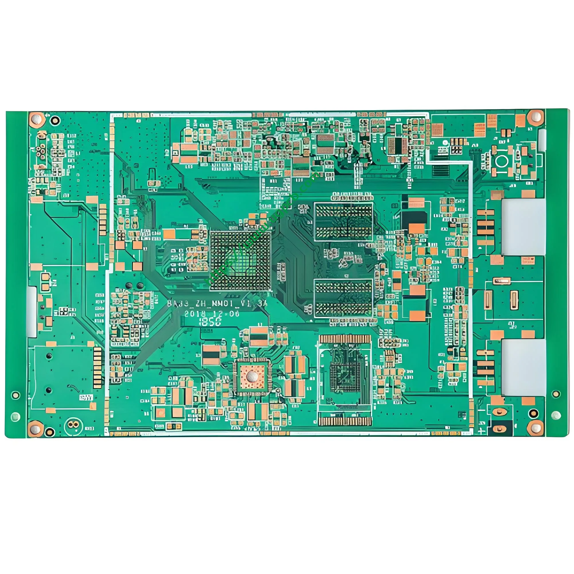
Visão geral do produto: O que é uma placa de circuito PCB antioxidante OSP?
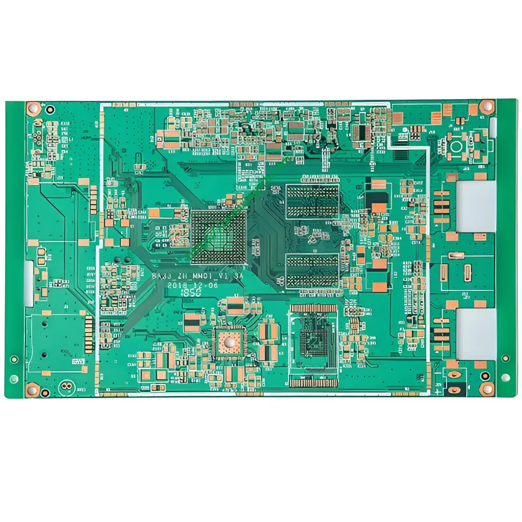
UmPlaca de circuito PCB antioxidante OSP usaConservantes orgânicos de soldabilidade (OSP) como seu acabamento superficial de cobre. Este processo deposita uma película orgânica ultrafina em superfícies de cobre nu. O filme evita a oxidação durante o armazenamento e montagem. Durante a soldagem, o fluxo dissolve rapidamente o filme OSP. Isso expõe cobre limpo para juntas de solda confiáveis.
A placa de circuito PCB antioxidante OSP da UGPCB usaLaminado epóxi de vidro FR-4 como material base. Possui 35μm (1 onças) Folha de cobre, 1.6espessura da placa mm, e dimensões de 68.36 × 34,6 mm. O tamanho mínimo do furo acabado é 0,45 mm. A largura mínima do traço é 0,15 mm e o espaçamento mínimo é 0,20 mm. O produto está em total conformidade com IPC-6012E (qualificação e desempenho de placa impressa rígida) e IPC-4555 (desempenho OSP em alta temperatura) especificações.
EssePCB OSP de dupla face atende eletrônicos de consumo, equipamento de comunicação, e controles industriais. Funciona melhor onde a sensibilidade ao custo e o nivelamento da superfície são mais importantes.
Classificação Científica de Produtos
Baseado em sistemas internacionais de classificação de PCB, este produto se enquadra nessas categorias:
| Dimensão de Classificação | Categoria |
|---|---|
| Material de substrato | PCB rígido de tecido de vidro epóxi FR-4 |
| Número de camadas | Frente e verso (circuito de duas camadas) |
| Acabamento superficial | OSP (Conservantes orgânicos de soldabilidade) antioxidante |
| Classificação inflamabilidade | UL 94 V-0 |
| Classe de desempenho IPC | Aula 2 (produtos eletrônicos de serviço dedicado) |
| Espessura da folha de cobre | 1 onças (35μm) cobre padrão |
| Espessura da placa | 1.6placa rígida padrão mm |
| Tipo de furo | Orifício passante compatível com SMT |
Principais parâmetros técnicos explicados
Substrato: Tecido de vidro epóxi FR-4
FR-4 é o substrato rígido mais comum no PCB indústria. “França” significa retardador de chama. “4” indica resina epóxi combinada com tecido de vidro que atendeUL 94 V-0 padrões de inflamabilidade. UL 94 V-0 requer que amostras verticais se autoextinguam dentro10 segundos após duas aplicações de chama de 10 segundos. Nenhuma gota de chama pode inflamar o algodão.

A temperatura de transição vítrea (Tg) mede a resistência ao calor. O padrão FR-4 Tg varia de 130–140°C. Mid-Tg FR-4 atinge 150–160°C. FR-4 de alta Tg excede 170°C. Este produto utiliza o padrão FR-4 com Tg ≥ 130°C (Compatível com IPC-4101/21). Isso atende às demandas de choque térmico da soldagem por refluxo (temperaturas de pico 240–260°C).
Espessura da folha de cobre: 35μm (1 onças)
A espessura do cobre determina a capacidade de transporte de corrente. Este produto utiliza35μm Folha de cobre, conhecido como1 onças de cobre (1 onças/pés² ≈ 35μm). De acordo com IPC-2221, 1 onças de cobre com aumento de temperatura de 10°C transportam aproximadamente:
- 0.15milímetros (6 mil) largura do traço: 0.5-0,7A
- 0.20milímetros (8 mil) largura do traço: 0.8-1,0A
A espessura de cobre de 35 μm é o padrão mais comum para PCBs de dupla face. Equilibra o custo, capacidade atual, e rendimento de fabricação.
Dimensões da placa: 68.36 × 34,6 mm
A placa acabada mede68.36mm × 34,6 mm. Este tamanho compacto é adequado para módulos eletrônicos compactos. PCBs pequenos exigem maior precisão – as tolerâncias dimensionais normalmente ficam dentro de ±0,15 mm (Classe IPC-6012 2).
Tamanho mínimo do furo acabado: 0.45milímetros
0.45milímetros é o furo passante mínimo revestido (PTH) diâmetro. Este tamanho de furo é um padrão na indústria. Garante um revestimento confiável (proporção de aspecto aproximadamente 3.6:1 com espessura de placa de 1,6 mm). O tamanho do furo acomoda a maioria dos componentes DIP e designs de almofadas SMT padrão.
Espessura da PCB: 1.6milímetros
1.6milímetros é a espessura de placa mais comum na fabricação de PCB. Proporciona excelente resistência mecânica e rigidez à flexão. Combina perfeitamente com conectores e soquetes padrão.
Largura e espaçamento do traço: 0.15milímetros / 0.20milímetros
Este produto oferecelargura mínima do traço de 0,15 mm (sobre 6 milésimos) eespaçamento mínimo de 0,20mm (sobre 8 milésimos). De acordo com a classificação IPC, essas dimensões se enquadramAula 2 (produtos eletrônicos de serviço dedicado). Esta precisão atende à maioria dos designs de PCB de média densidade, incluindo placas de controle MCU, módulos de gerenciamento de energia, e placas conversoras de interface.
Como funciona o processo antioxidante OSP
O processo OSP desenvolve uma película orgânica ultrafina em cobre puro e limpo através deadsorção química. O filme OSP consiste principalmente emcompostos de alquil benzimidazol (à base de azol). A espessura do filme normalmente varia de0.2–0,5μm.
Mecanismo de Proteção
O filme OSP protege as superfícies de cobre através de três mecanismos:
- Barreira física – O filme orgânico forma uma camada molecular densa. Ele impede que o oxigênio e a umidade entrem em contato com a superfície do cobre.
- Adsorção química – Grupos ativos em moléculas OSP ligam-se quimicamente com átomos de cobre. Isso cria uma forte adesão.
- Proteção seletiva – O filme OSP cobre apenas áreas de cobre. Não afeta a máscara de solda ou outras regiões não metálicas.
Comportamento durante a soldagem
Durante o refluxo SMT, temperaturas atingem190–230ºC. Os ingredientes ativos do fluxo decompõem e dissolvem o filme OSP. Isso expõe cobre limpo por baixo. A solda entra em contato direto com o cobre nu e formacompostos intermetálicos (CMI). Isso cria conexões elétricas confiáveis. O filme OSPse decompõe completamente sem nenhum resíduo após a soldagem.
Principais características de desempenho
Baseado nos métodos de teste IPC-TM-650:
| Característica | Valor típico / Exigência | Padrão de Referência |
|---|---|---|
| Espessura do filme OSP | 0.2–0,5μm | IPC-4555 |
| Ângulo de molhamento da solda | ≤30° (depois 1 reflow) | IPC-TM-650 2.4.1 |
| Taxa de propagação de solda | ≥80% | IPC-TM-650 2.4.1 |
| Proteção contra oxidação (ambiente) | ≥6 meses | IPC-4555 |
| Mudança de resistência de contato | ≤10% (depois 6 meses de armazenamento) | IPC-TM-650 |
Processo de fabricação de PCB antioxidante OSP
A fabricação de PCB antioxidante OSP segue controles de processo rigorosos. Cada etapa afeta a qualidade e a confiabilidade finais.
Processos front-end (Preparação de substrato & Padronização de circuito)
- Corte de materiais – Corte o laminado revestido de cobre FR-4 no tamanho certo
- Perfuração – Perfuração CNC com tamanho mínimo de furo de 0,45 mm
- Cobre sem eletricidade / Galvanoplastia – Metalizar paredes de furos para conexão camada a camada
- Transferência de padrão de circuito – Filme seco / exposição e revelação de filme úmido
- Gravura – Remova o cobre indesejado para criar um traço de 0,15 mm / 0.20circuito de espaçamento mm
- Impressão de máscara de solda – Aplique tinta de máscara de solda verde ou de outra cor
- Pré-limpeza – Remova óxidos e contaminantes antes do acabamento da superfície
Processo de revestimento OSP (Processo Central)
O fluxo típico de revestimento OSP:
Desengorduramento → Enxágue duplo com água → Micro-gravação → Enxágue duplo com água → Decapagem ácida → Enxágue com água DI → Formação de filme OSP → Secagem ao ar → Enxágue com água DI → Secagem final
- Micro-Gravação – Remove óxidos de cobre e cria uma superfície microscopicamente áspera e uniforme. Isso promove o crescimento do filme OSP.
- Formação de Filme OSP – Mergulhe o PCB na química OSP (alquil benzimidazol, ácidos orgânicos, cloreto de cobre, e água deionizada). O filme cresce através de adsorção química em superfícies de cobre.
- Controle de espessura do filme – O controle preciso é crítico. Muito fino significa baixa resistência ao calor. Muito grosso prejudica a ação do fluxo e o fluxo da solda.
Processos de back-end
- Roteamento – Roteamento CNC até as dimensões finais
- Teste elétrico – Sonda voadora ou teste de fixação
- Inspeção Final – Inspeção visual e amostragem de espessura de filme
- Embalagem a vácuo – Embalagem à prova de umidade e oxidação
Recursos do produto e principais vantagens
Excelente planicidade de superfície
O filme OSP é apenas0.2–0,5μm espesso. Forma-se através de adsorção química com espessura uniforme e superfície lisa. Isso preserva o nivelamento original da folha de cobre. É ideal paraSMT de passo fino componentes (como 0,4 mm e abaixo do passo QFP, Pacotes QFN).
Soldabilidade superior
O filme OSP se dissolve rapidamente no fluxo durante o refluxo. Isso expõe cobre fresco para formação confiável de IMC. O processo OSP suporta tantofuro passante (THT) emontagem em superfície (SMT) de solda.
Econômico
OSP não utiliza metais preciosos (ouro, prata, paládio). Os custos de material e processamento são inferiores aos do ENIG, prata de imersão, ou lata de imersão. Para produção de alto volume, como produtos eletrônicos de consumo, OSP oferece competitividade de custos excepcional.
Ambientalmente compatível
OSP usa compostos orgânicos. Não contém chumbo, mercúrio, cádmio, ou cromo hexavalente. Atende plenamenteRoHS 2.0 requisitos. Os custos e a complexidade do tratamento de resíduos também são inferiores aos dos processos de acabamento metálico.
Tempo de processamento curto
O revestimento OSP é simples e rápido. Não necessita de equipamentos de galvanização complexos ou longos tempos de deposição. Comparado com ENIG (que leva horas), OSP conclui acabamento superficial em30–60 minutos por lote. Isto reduz significativamente os prazos de entrega.
Diretrizes de design e considerações importantes
Design para Fabricação (Dfm) Regras
Com base nas capacidades de processo deste produto:
| Parâmetro de projeto | Capacidade do produto | Valor de projeto recomendado |
|---|---|---|
| Largura mínima de traços | 0.15milímetros | ≥0,15 mm (traços de sinal) |
| Espaçamento Mínimo | 0.20milímetros | ≥0,20 mm |
| Tamanho mínimo do orifício | 0.45milímetros | ≥0,45 mm |
| Espessura da placa | 1.6milímetros | 1.6milímetros (padrão) |
Limitações e mitigações do processo OSP
OSP oferece muitos benefícios, mas tem limitações inerentes:
- Vida útil limitada – O filme OSP protege para6 meses em condições ambientais. Para melhor soldabilidade, montagem SMT completa dentro 3 meses.
- Sensibilidade à umidade – Filmes OSP degradam em alta temperatura, ambientes de alta umidade. Armazene as placas em20–25°C com 40–60% de umidade relativa.
- Ciclos de refluxo limitados – OSP padrão suporta1–2 refluxo choques térmicos. Vários refluxos requerem OSP de alta temperatura (Compatível com IPC-4555).
- Desafios de testes elétricos – O filme OSP é isolante. Afeta a confiabilidade do contato de teste elétrico. Os pontos de teste precisam de impressão em pasta de solda para remover a camada OSP.
Recomendações de armazenamento e manuseio
- Embalagem selada a vácuo com dessecante e cartões indicadores de umidade
- Ambiente de armazenamento: temperatura ≤30°C, umidade relativa ≤60%
- Soldagem completa dentro48 horas de abrir o pacote
- Use luvas antiestáticas durante o manuseio. Evite o contato das mãos nuas com as superfícies da placa.
Cenários de aplicação típicos
As placas de circuito PCB antioxidante OSP atendem a muitas indústrias devido à suavantagem de custo, planicidade da superfície, e excelente soldabilidade:
Eletrônicos de consumo
- Placas-mãe de smartphones e PCBs de tablets
- Placas-mãe de computador e placas gráficas
- Painéis de controle de eletrodomésticos
- Placas de circuito de dispositivos vestíveis
Equipamento de comunicação
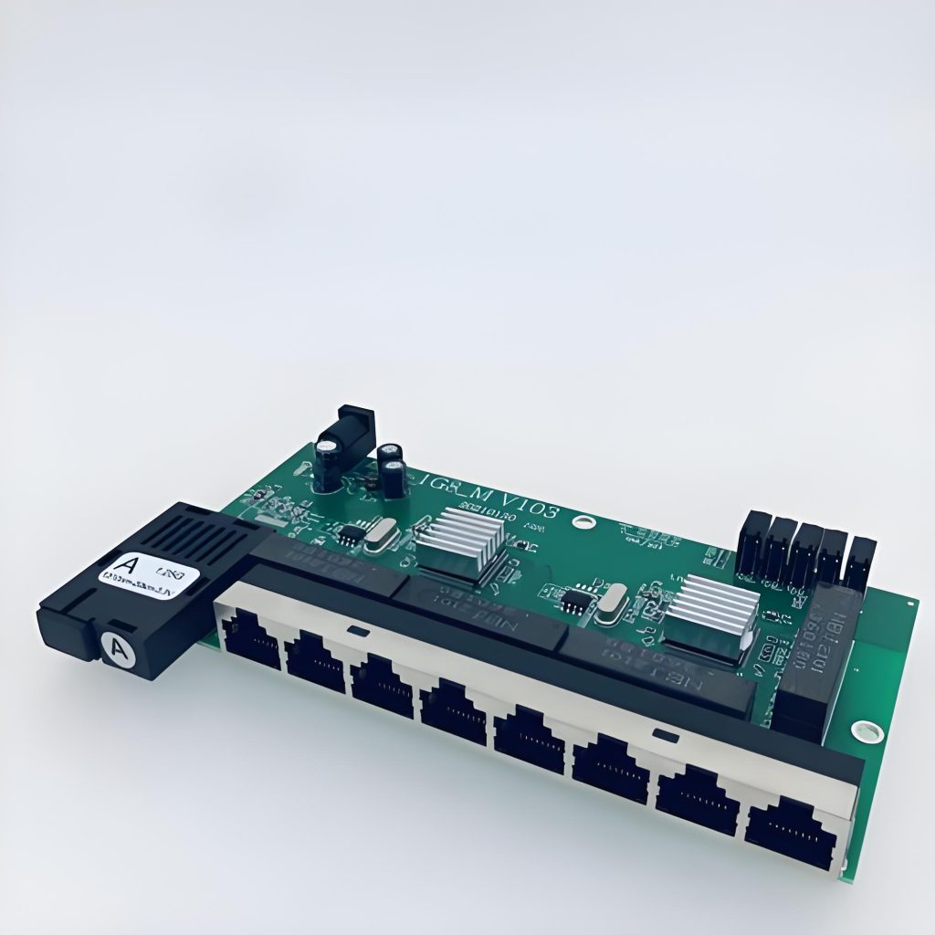
- PCBs de roteadores e switches
- Módulos de comunicação e dispositivos IoT
- Bluetooth / Placas portadoras de módulo Wi-Fi
Controles Industriais
- Controladores lógicos programáveis PLC
- Módulos de gerenciamento de energia
- Placas de circuito de instrumentação
- Placas de controle de acionamento de motor
Eletrônica Automotiva (Não crítico para a segurança)
- Sistemas de infoentretenimento no veículo
- Módulos de controle corporal
- Placas de interface de sensores
Garantia de qualidade e conformidade com padrões
Padrões Aplicáveis
O produto PCB antioxidante OSP da UGPCB segue estritamente esses padrões internacionais:
| Padrão | Título | Escopo |
|---|---|---|
| IPC-4555 | Especificação de desempenho para conservantes orgânicos de soldabilidade em alta temperatura (OSP) para placas impressas | Requisitos e testes de processo OSP |
| IPC-6012E | Especificação de qualificação e desempenho para placas impressas rígidas | Qualidade e desempenho da placa acabada |
| IPC-4101/21 | Especificação para laminado epóxi reforçado com vidro | Requisitos técnicos do substrato FR-4 |
| IPC-TM-650 | Manual de Métodos de Teste | Vários métodos de teste de desempenho |
| UL 94 V-0 | Inflamabilidade de Materiais Plásticos | Segurança retardante de chama do substrato |
| RoHS 2.0 | Restrição de Substâncias Perigosas | Conformidade ambiental |
Principais indicadores de qualidade
De acordo com os requisitos do IPC, as principais métricas de qualidade incluem:
- Espessura do filme OSP: 0.2–0,5μm, tolerância de uniformidade ≤ ±0,1μm
- Adesão: ≥4B (IPC-TM-650 2.4.29 teste de corte transversal)
- Taxa de propagação de solda: ≥80% (IPC-TM-650 2.4.1)
- Período de proteção contra oxidação: ≥6 meses (condições ambientais)
- Classificação inflamabilidade: UL 94 V-0
Por que escolher UGPCB para PCBs antioxidantes OSP?
Capacidades de fabricação de precisão
- 0.15mm largura mínima do traço / 0.20espaçamento mínimo mm
- 0.45mm tamanho mínimo do furo acabado
- 1.6mm de espessura padrão da placa com excelente compatibilidade
Controle confiável de processos OSP
- Aderência estrita ao IPC-4555 para espessura e qualidade do filme
- Rastreabilidade total durante todo o processo de fabricação
- Testes de soldabilidade e amostragem de espessura de filme para cada lote
Entrega rápida
- Prazo de entrega padrão: 7–10 dias úteis
- Suporta amostragem de protótipo e produção em volume
Suporte Técnico Abrangente
- Revisão gratuita do projeto DFM
- Equipe de engenharia profissional para orientação de seleção de produtos
Faça uma cotação hoje
UGPCB oferece soluções de placa de circuito PCB antioxidante OSP de alto valor. Se você precisaamostragem de protótipo ouprodução em volume, oferecemos suporte técnico profissional e preços competitivos.
📞 Como obter um orçamento:
- Envie seus arquivos Gerber e lista BOM
- Nossa equipe de engenharia responde com uma solução personalizada e orçamento dentro24 horas
- Verificação DFM gratuita para garantir que seu projeto seja aprovado na primeira vez
Declaração da fonte de dados: Os dados técnicos e requisitos padrão citados neste documento são derivados principalmente do IPC (Associação conectando indústrias eletrônicas) padrões incluindo IPC-4555 “Especificação de desempenho para conservantes orgânicos de soldabilidade em alta temperatura (OSP) para placas impressas,” IPC-6012E “Especificação de qualificação e desempenho para placas impressas rígidas,” IPC-4101/21 “Especificação para laminado epóxi reforçado com vidro,” IPC-TM-650 “Manual de Métodos de Teste,” e UL 94 “Norma para Testes de Inflamabilidade de Materiais Plásticos para Peças em Dispositivos e Eletrodomésticos.” Alguns parâmetros de processo fazem referência a dados técnicos disponíveis publicamente dos principais fabricantes de PCB. Todos os dados foram verificados quanto à precisão.













