

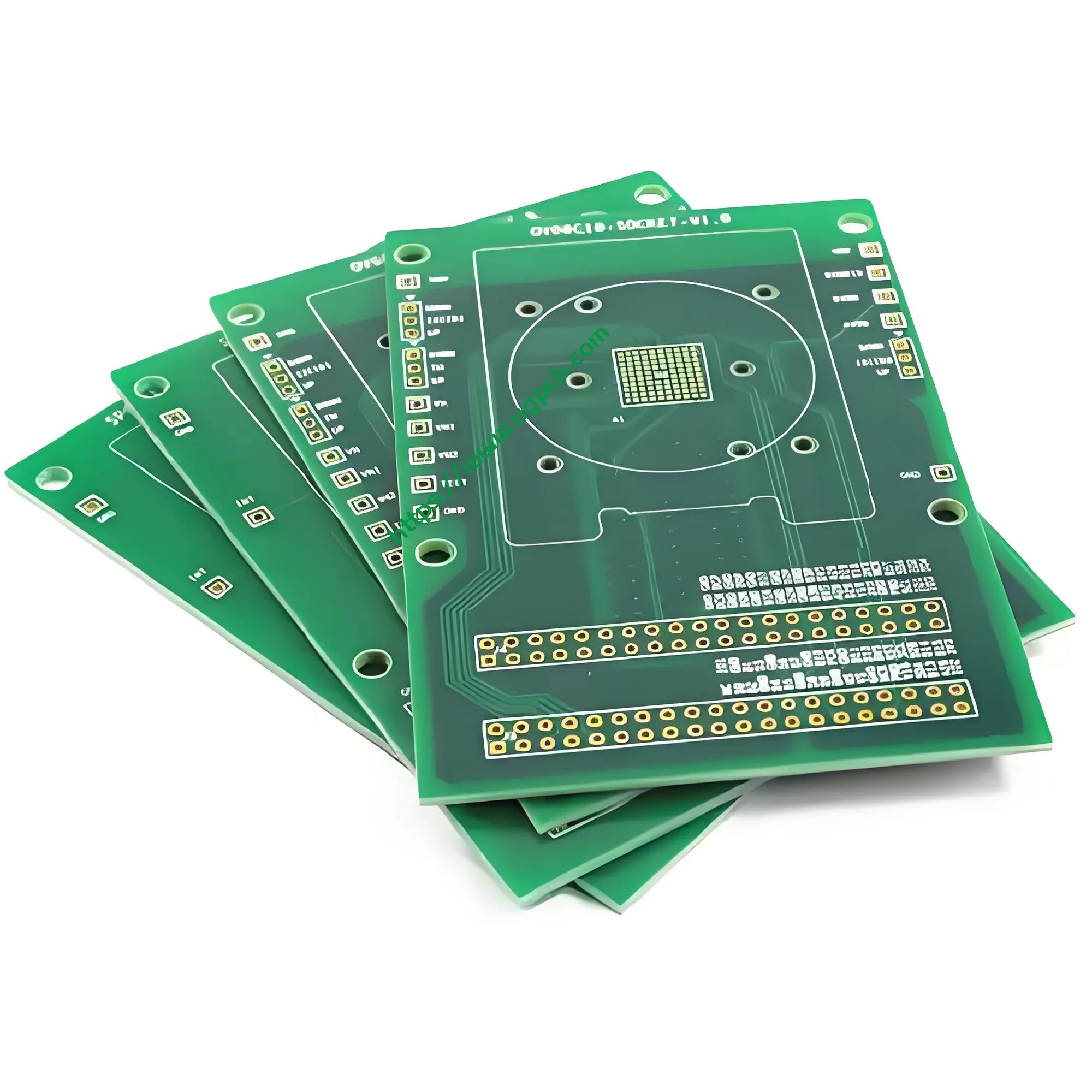
1. Visão geral do produto: O que é um PCB de aspirador de pó sem fio?
Um aspirador de pó sem fio PCB (Placa de circuito impresso) é o principal componente eletrônico responsável pelo controle do acionamento do motor, gerenciamento de energia, interação do usuário, e proteção de segurança dentro de um aspirador sem fio. Em termos simples, serve como “cérebro” e “centro nervoso” do dispositivo. Recebe comandos de botão, controla a velocidade do motor sem escova, gerencia o carregamento e descarregamento da bateria, monitora o status operacional, e implementa múltiplas proteções de segurança.
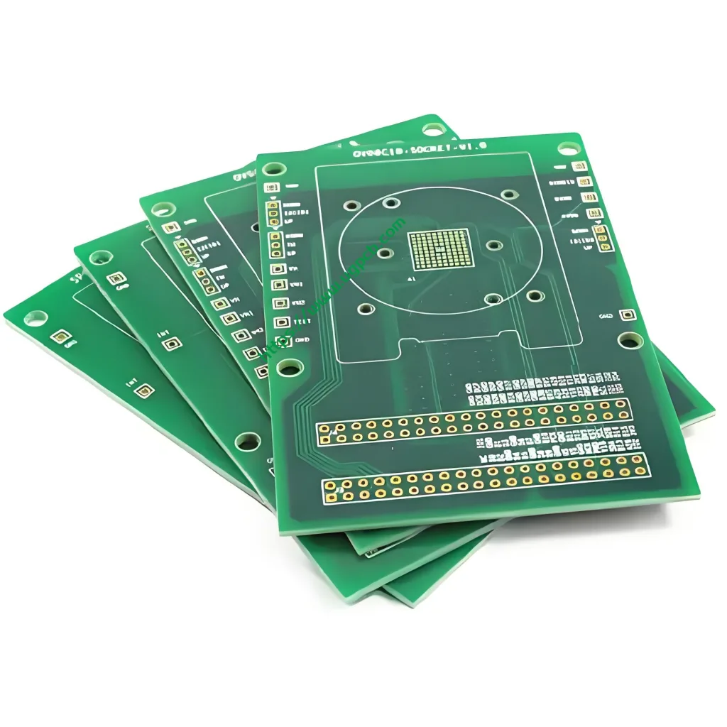
UGPCB apresenta este PCB de aspirador de pó sem fio - um 2-placa de circuito impresso rígida de camada projetado especificamente para equipamentos de limpeza portáteis. Ele usa Laminado revestido de cobre epóxi de vidro FR-4 como material base. A espessura da placa é de 1,0 mm, e as dimensões são 86.37 × 72,6 mm. Este tamanho compacto cabe perfeitamente nos espaços internos apertados de aspiradores sem fio portáteis e tipo bastão.
Por IPC-6012F Especificação de qualificação e desempenho para placas impressas rígidas, este produto se enquadra no placa impressa dupla face rígida (com furos banhados) categoria. Como parte fundamental do balcão único da UGPCB PCB soluções, este produto atende aos padrões internacionais do IPC desde o projeto até a fabricação e controle de qualidade. Ele fornece aos fabricantes de aspiradores uma alta confiabilidade, econômico PCBA solução.
2. Classificação do Produto: Posicionamento Científico e Categorização da Indústria
Por IPC-6012F e PCB padrão sistemas de classificação da indústria, este produto pode ser cientificamente categorizado da seguinte forma:
| Dimensão de Classificação | Categoria |
|---|---|
| Por estrutura | Placa rígida impressa frente e verso (com furos banhados) |
| Por material base | Laminado revestido de cobre e vidro tecido epóxi FR-4 (compatível com IPC-4101) |
| Por contagem de camadas | 2-placa de camada (PCB de dupla face) |
| Por acabamento superficial | HASL sem chumbo (Nivelamento de solda com ar quente) |
| Por classificação de inflamabilidade | UL 94 V-0 |
| Por aplicação | Eletrônica de consumo / placa de controle de pequenos eletrodomésticos (aspirador PCBA) |
Dentro da indústria eletrônica de aspiradores de pó, este produto pertence aoacionamento e controle do motor PCBA categoria. Juntamente com a placa de controle principal e a placa de gerenciamento de energia, ele forma os três módulos de circuito principais de um aspirador sem fio.
3. Principais parâmetros técnicos
3.1 Material base e espessura da placa
- Material base: FR-4 (laminado revestido de cobre epóxi reforçado com fibra de vidro)
- Espessura da placa: 1.0milímetros
FR-4 é o substrato rígido mais utilizado na indústria de PCB. Para IPC-4101, FR-4 oferece excelente isolamento elétrico, força mecânica, e resistência ao calor. O padrão FR-4 tem uma temperatura de transição vítrea (Tg) de 130–140°C. Para IPC-6012, a faixa de tolerância para espessura de placa de 1,0 mm é de ± 0,1 mm.
3.2 Contagem e dimensões de camadas
- Contagem de camadas: 2 camadas (placa de dupla face)
- Dimensões: 86.37 × 72.6 milímetros
A estrutura de 2 camadas controla efetivamente os custos de fabricação, ao mesmo tempo em que oferece desempenho elétrico sólido. Isso o torna a escolha principal para placas de controle de aspiradores sem fio. O compacto 86.37 × As dimensões de 72,6 mm são otimizadas para o espaço limitado dentro dos aspiradores.
3.3 Largura/espaçamento do traçado e tamanho mínimo do furo
- Tamanho mínimo do orifício: 0.45milímetros
- Largura/espaçamento do traçado: 0.45milímetros / 0.391milímetros
Por IPC-2221CPadrão genérico para design de placas impressas, a largura do traço e o projeto do espaçamento devem considerar o desempenho elétrico, capacidade de transporte de corrente, e capacidade de fabricação. O tamanho mínimo do furo de 0,45 mm suporta soldagem confiável de componentes DIP convencionais e peças de furo passante.
Para capacidade de transporte de corrente, a fórmula padrão da indústriaEu = k·ΔT^0,44·A^0,725 (onde A é a área da seção transversal do traço) mostra que com 1 onça de cobre, um 0,45 mm (aprox.. 18mil) o traço pode transportar cerca de 1,8–2,0A. A PCB do aspirador sem fio usa essa largura de traço para sinais de acionamento do motor e sinais de controle, garantindo uma operação estável a longo prazo.
3.4 Espessura da folha de cobre
- Espessura da folha de cobre: 1/1 OZ (1 onça em ambas as camadas externas)
1onça de folha de cobre (aprox.. 35μm) é a configuração padrão para PCBs de eletrônicos de consumo. Ele atinge um excelente equilíbrio entre a capacidade de transporte de corrente, condutividade térmica, e custo.
3.5 Acabamento superficial
- Acabamento superficial: HASL sem chumbo (Nivelamento de solda com ar quente)
HASL é um acabamento de superfície de PCB maduro e econômico. HASL sem chumbo atende aos requisitos ambientais RoHS. De acordo com os padrões IPC, HASL sem chumbo normalmente tem uma espessura de camada de estanho de 1–40μm, com processos convencionais controlados em 5–25μm. Este acabamento oferece excelente soldabilidade (molhabilidade) e uma boa vida útil de armazenamento de até 12 meses.
3.6 Máscara de solda e legenda
- Cor da máscara de solda: Tinta verde
- Cor da legenda: Branco
A máscara de solda verde é a escolha mais popular da indústria. Fornece excelente proteção de isolamento e alto contraste para AOI (Inspeção óptica automatizada). As legendas brancas são claras e fáceis de ler, facilitando a colocação de componentes e manutenção futura.
4. Diretrizes de projeto: Seguindo os padrões IPC-2221C
Um PCB de aspirador de pó sem fio bem projetado deve seguir estes princípios básicos (por IPC-2221C):
4.1 Projeto de Desempenho Elétrico
- Largura do rastreamento de energia: Calcule usando a fórmula Eu = k·ΔT^0,44·A^0,725 para garantir que o aumento da temperatura permaneça abaixo de 10°C na corrente operacional máxima.
- Integridade do sinal: Use largura de traço de 0,45 mm para sinais de controle para garantir a transmissão completa de sinais de controle de velocidade PWM e sinais de sensor.
- Projeto de aterramento: Use estratégias de aterramento de ponto único ou de aterramento dividido para evitar interferência do circuito de potência com o circuito de controle.
4.2 Projeto de gerenciamento térmico
Os aspiradores sem fio geram calor significativo dos MOSFETs durante a operação. O Projeto de PCB deve resolver isso por:
- Colocação térmica por meio de matrizes sob dispositivos de energia.
- Ampliando traços de alta corrente ou adicionando cobre exposto para melhor dissipação de calor.
- Usando placa de espessura de 1,0 mm para equilibrar condutividade térmica e resistência mecânica.
4.3 Projeto de Estrutura Mecânica
O 86.37 × As dimensões de 72,6 mm devem corresponder exatamente à caixa do aspirador. As posições dos furos de montagem e os locais dos conectores devem atender aos requisitos do projeto estrutural. O tamanho mínimo do furo de 0,45 mm suporta soldagem através do furo para vários componentes e conectores DIP.
5. Princípio de funcionamento
O PCB do aspirador sem fio opera por meio dos seguintes processos principais:
① Entrada e gerenciamento de energia: A bateria de lítio (normalmente 21,6 V ou 25,2 V) passa pelo circuito de gerenciamento de energia no PCB. Isso fornece tensões estáveis para o chip de controle principal e circuitos de driver.
② Computação do chip de controle principal: O MCU (microcontrolador) no PCB recebe comandos de botão. Ele calcula e emite sinais de acionamento trifásicos usando FOC (Controle Orientado a Campo) ou algoritmos de controle de onda quadrada.
③ Acionamento do motor: Os sinais de acionamento são amplificados por dispositivos de potência MOSFET. Esses sinais então acionam o motor DC sem escova (BLDC) girar em alta velocidade, gerando o fluxo de ar necessário para sucção.
④ Feedback e Proteção: A PCB monitora continuamente a corrente do motor, tensão da bateria, temperatura, e outros parâmetros. Quando detecta condições anormais, como sobrecorrente, temperatura excessiva, subtensão, ou bloqueio do rotor, ele executa imediatamente ações de proteção.
6. Materiais utilizados
| Componente | Material | Descrição |
|---|---|---|
| Substrato | Vidro epóxi FR-4 | Compatível com IPC-4101 |
| Camada Condutiva | Folha de cobre eletrolítica (1onças) | 1onças em ambas as camadas externas |
| Máscara de solda | Tinta fotoimageável verde | Proteção de isolamento, resistência à oxidação |
| Acabamento superficial | Liga HASL sem chumbo | Compatível com RoHS |
| Tinta Legenda | Tinta epóxi branca | Alto contraste, resistente ao calor |
O substrato FR-4 carrega um UL 94 V-0 Classificação inflamabilidade. No teste de queima vertical, a chama se apaga dentro 10 segundos após a remoção, sem gotas ardentes. Este recurso é crítico para alta potência, dispositivos alimentados por bateria, como aspiradores de pó sem fio. Reduz significativamente o risco de incêndio causado por falhas no circuito.
7. Especificações de desempenho
7.1 Desempenho elétrico
| Parâmetro | Especificação | Padrão de Referência |
|---|---|---|
| Resistência de Isolamento | ≥10 ^ 6 MΩ | IPC-6012F |
| Tensão suportável dielétrica | Até 500 V (dependente do design) | IPC-2221C |
| Resistência de condução | ≤50mΩ (típico) | IPC-6012F |
| Impedância Característica | Controlável mediante solicitação (50Ω/90Ω/100Ω) | IPC-2221C |
7.2 Desempenho térmico
| Parâmetro | Especificação | Padrão de Referência |
|---|---|---|
| Temperatura de transição vítrea (Tg) | ≥135°C (Método DSC) | IPC-TM-650 2.4.25 |
| Resistência ao calor da solda | 288°C / 10s, Sem delaminação | IPC-4101 |
| Zis Z CTE (CTEz) | ≤65 ppm/°C (50–260ºC) | IPC-4101 |
7.3 Desempenho Mecânico
| Parâmetro | Especificação | Padrão de Referência |
|---|---|---|
| Tolerância de espessura da placa | ±0,1 mm | IPC-6012 |
| Tolerância do tamanho do furo | ± 0,05 mm | IPC-6012F |
| Classificação inflamabilidade | UL 94 V-0 | UL 94 |
7.4 Confiabilidade
- Teste de soldabilidade: Compatível com IPC-J-STD-003
- Teste de envelhecimento: 500 horas sob condições double-85 (85°C / 85%RH) sem anormalidades
8. Características estruturais
8.1 2-Vantagens da placa de camada
A camada superior carrega os principais componentes e traços de sinal. A camada inferior lida com componentes auxiliares e derramamentos de cobre de aterramento/energia. O design de 2 camadas alcança omelhor custo emaior confiabilidade equilíbrio para funções de controle de aspirador sem fio.
8.2 Orifício revestido (PTH) Processo
Todos os furos passantes usam o processo de furo passante. Isso garante uma interconexão confiável entre as camadas superior e inferior. Ele também fornece suporte mecânico sólido e conexão elétrica para componentes DIP.
8.3 Processo de ponte de máscara de solda
A máscara de solda verde forma pontes entre as almofadas adjacentes. Isso evita curtos-circuitos de soldagem e melhora o rendimento de colocação de SMT.
9. Fluxo do Processo de Fabricação
A UGPCB segue rigorosamente os padrões IPC-6012F para controlar todas as etapas da produção:
① Inspeção de materiais recebidos →② Criação de circuito de camada interna (para placas de 2 camadas, esta é diretamente a camada externa) →③ Laminação (não aplicável para placas de 2 camadas) →④ Perfuração (tamanho mínimo do furo 0,45 mm) →⑤ Deposição de cobre sem eletricidade / Chapeamento de painel →⑥ Circuito da Camada Externa →⑦ Revestimento padrão →⑧ Gravura →⑨ Máscara de solda (tinta verde) →⑩ Acabamento de superfície (HASL sem chumbo) →⑪ Legenda (personagens brancos) →⑫ Roteamento de perfil (86.37 × 72,6 mm) →⑬ Teste Elétrico →⑭ Inspeção Final (para IPC-A-600) →⑮ Embalagem e envio
Cada lote sofreteste de sonda voadora outeste de fixação dedicado para garantir 100% sem circuitos abertos ou em curto.
10. Cenários de aplicação
10.1 Aplicações primárias
- Aspiradores portáteis sem fio: Acionamento e controle do motor em espaços compactos
- Aspiradores sem fio estilo bastão: Gerenciamento de bateria e acionamento de motor sem escova
- Aspiradores robóticos: Controle de navegação e acionamento motorizado
- Aspiradores de carro: 12Adaptação e controle de energia V/24V
- Dispositivos de limpeza inteligentes: Conectividade IoT e controle inteligente
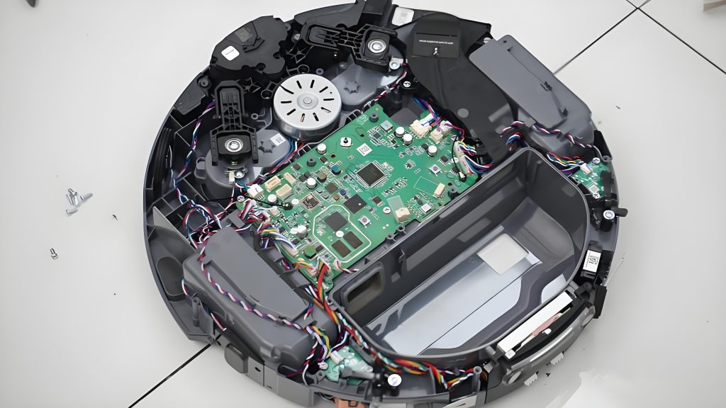
10.2 Exemplos de produtos finais
Este PCB pode ser amplamente utilizado em placas de controle e drivers para aspiradores sem fio e dispositivos de limpeza semelhantes de marcas como Xiaomi, Dyson, Tineco, e Leifheit.
11. Por que escolher o PCB do aspirador de pó sem fio da UGPCB?
✅Conformidade com Padrões Internacionais: Projeto, fabricação, e inspeção estão em total conformidade com IPC-6012F, IPC-A-600, IPC-2221C, e outras normas internacionais
✅UL 94V-0 Segurança contra incêndio: O substrato FR-4 atinge a mais alta classificação de queima vertical, garantindo a segurança do dispositivo

✅Processo ecológico sem chumbo: O acabamento superficial HASL sem chumbo atende às diretivas ambientais RoHS e REACH
✅Capacidade de fabricação comprovada: UGPCB fornece serviços completos, desde o projeto e fabricação de PCB até a montagem de PCBA
✅Rigoroso controle de qualidade: Inspeção visual conforme IPC-A-600 e 100% testes elétricos garantem a qualidade da remessa
✅Dimensões Compactas Otimizadas: O 86.37 × O tamanho de 72,6 mm se adapta perfeitamente ao espaço interno de vários aspiradores sem fio
12. Obtenha um orçamento e amostras hoje
UGPCB está empenhada em fornecer alta precisão, soluções PCB e PCBA de alta confiabilidade para fabricantes de eletrônicos em todo o mundo. Se você precisa PCBs nus, PCBA totalmente montado, ou serviços completos, desde o design até a produção em massa, UGPCB tem experiência para apoiá-lo.
📧Contate a UGPCB para um orçamento personalizado hoje →
- Site: www.ugpcb.com
- Modificações e otimizações de design personalizadas disponíveis
- DFM grátis (Design para fabricação) análise
- Prototipagem rápida e produção em volume disponíveis
Declaração de fonte de dados
Os padrões técnicos e dados citados neste artigo vêm das seguintes organizações autorizadas:
- IPC (Associação conectando indústrias eletrônicas): IPC-6012F Especificação de qualificação e desempenho para placas impressas rígidas, IPC-A-600 Aceitabilidade de placas impressas, IPC-2221C Padrão genérico para design de placas impressas, IPC-4101 Especificação de materiais básicos para placas impressas rígidas e multicamadas, IPC-TM-650 Manual de Métodos de Teste
- UL (Laboratórios de subscritores): UL 94 Norma para Segurança de Inflamabilidade de Materiais Plásticos para Peças em Dispositivos e Eletrodomésticos –V-0 avaliação
- Fórmula de engenharia padrão da indústria: Fórmula de capacidade de transporte de corrente de PCB Eu = k·ΔT^0,44·A^0,725













