
Введение
Гибкие печатные платы (FPCS) стали незаменимыми в складных смартфонах, носимые устройства, и аэрокосмическая электроника из-за их ультратонкого профиля и сгибаемой природы. Однако, Сложность их дизайна превосходит традиционную жесткую печатные платы, Требование междисциплинарного опыта в области материаловедения, механическое моделирование, и процесс инноваций. Это всеобъемлющее руководство исследует критические аспекты гибких дизайн печатной платы Через проверенные отрасли методологии и передовые технологии.
1. Материальная наука: Фонд гибких печатных плат
1.1 Выбор субстрата: Баланс производительности и стоимости
Гибкие субстраты должны одновременно достигать тепловой стабильности (> 260 ° C для PI против < 120 ° C для ПЭТ), изгибая выносливость, и диэлектрические свойства. Полиимид (ПИ) доминирует в высококлассных приложениях с его низким CTE (≈12 ч/млн/℃), Пока полиэстер (ДОМАШНИЙ ПИТОМЕЦ) обслуживает чувствительные к стоимости статические приложения. Новые подложки PI с низким содержанием модулей (< 3 GPA) Включить динамическую изгибную прочность на миллион циклов.
Техническая формула:
Расчет стресса изгиба:
S = (E · T.)/(2Р)
Где e = упругой модуль, Т = толщина, R = радиус изгиба. Уменьшение E или увеличение r снижает концентрацию стресса на 62%.
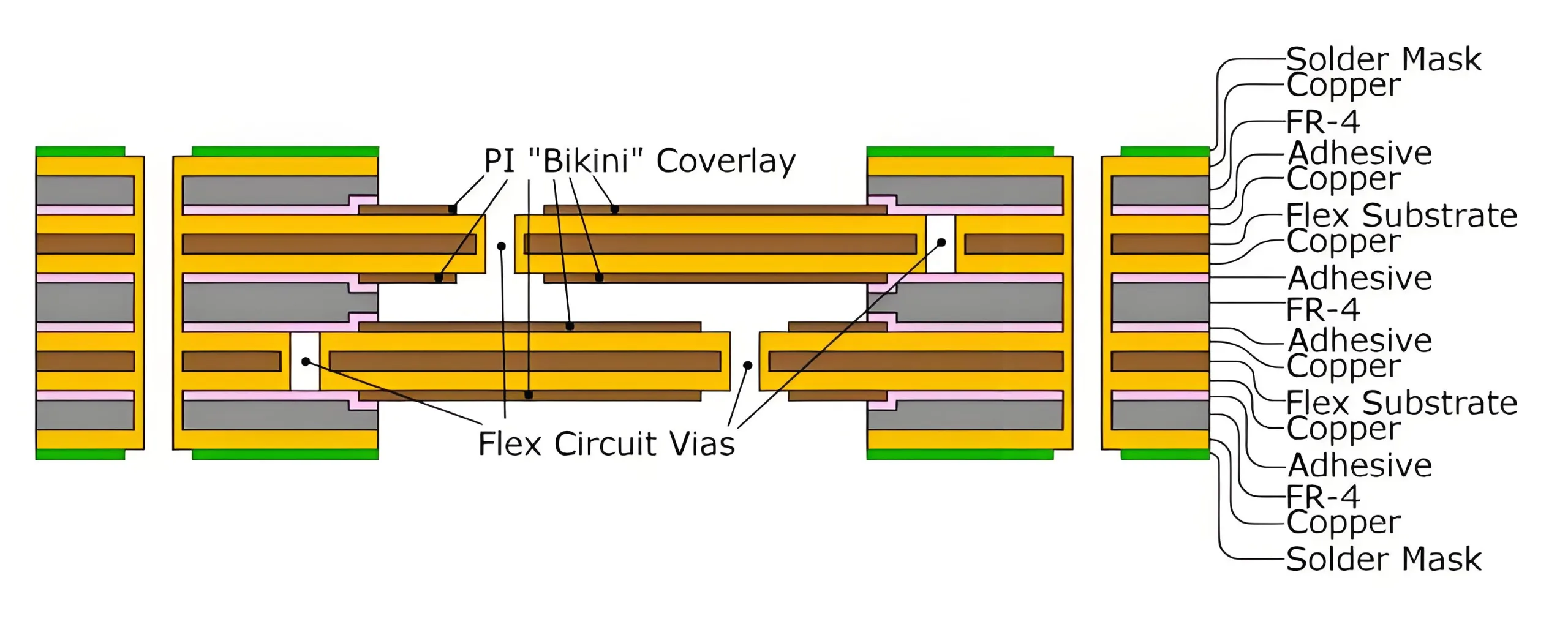
1.2 Медная фольга и покрываем: Механическая гармония
Обмороженный (Раствор) медная фольга улучшает пластичность 30% над электродепоснуто (Редакция) Фольга в динамических зонах изгиба. Оптимальная покрывалка сочетает в себе акриловый клей (15-25мкм) с пленкой PI для сбалансированной адгезии и гибкости.
1.3 Защитный слой инновации
Сетчатые заземления и дугообразное медное подкрепление (≥0,2 мм ширина) уменьшить риски разрыва 70% в уязвимых областях, таких как золотые пальцы. Enig или OSP+селективное покрытие золота обеспечивает надежную пайку.
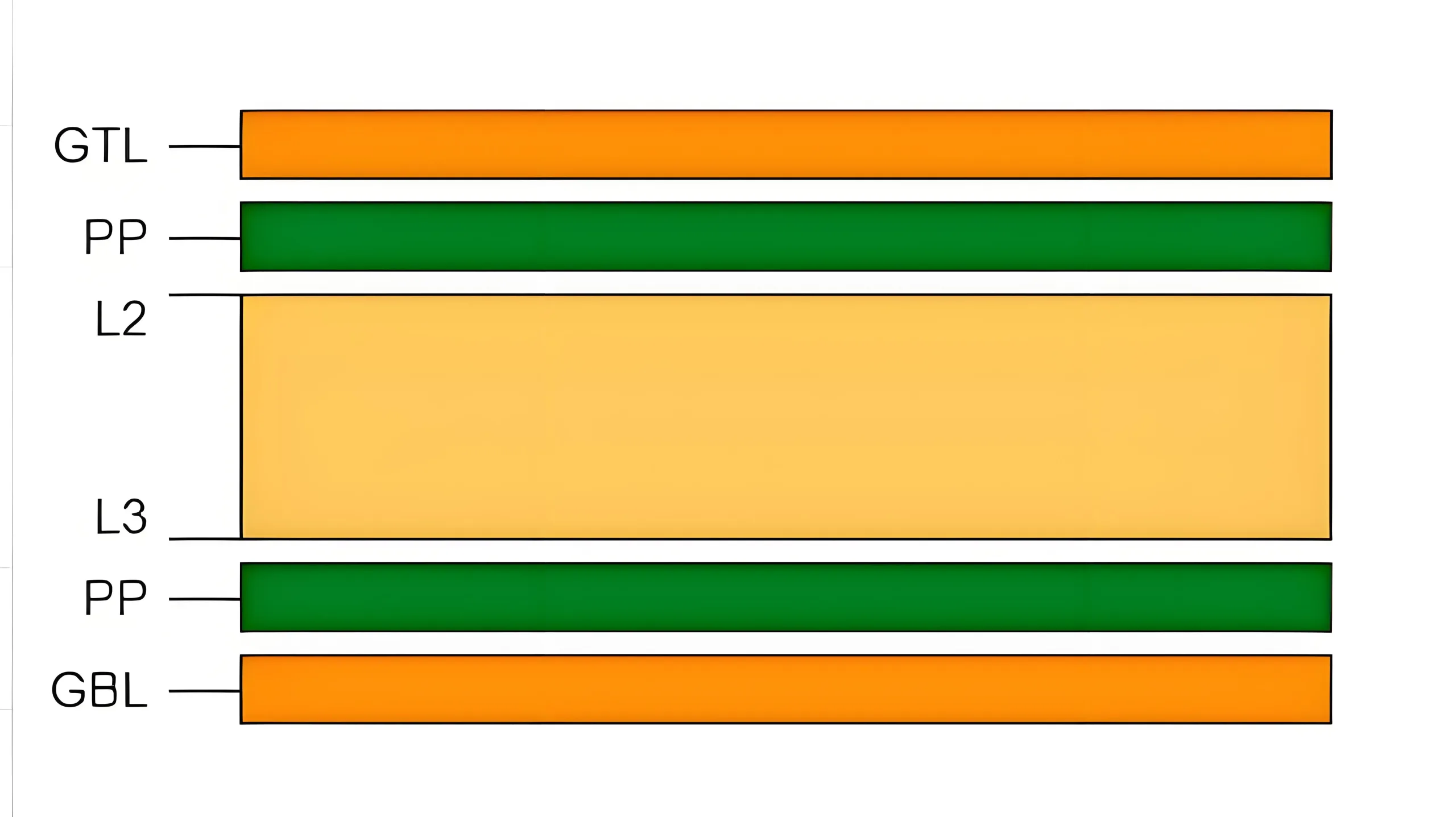
2. Архитектура стека: Инженерная жесткая синергия
2.1 Стандартизация слоя и целостность сигнала
-
Слои сигнала: Центральное позиционирование сводит к минимуму EMI
-
Силовые плоскости: Сплошная медь (< 50 МОм -целевой импеданс)
-
Наземные слои: Сетчатые узоры (≤5 мм расстояние) уменьшить зоны петли
Тематическое исследование: 8-Уровень жесткой платы с жесткой фиксацией с конфигурацией 2R+4F+2R достигает достижения 100,000+ циклы изгиба.
2.2 Зоны перехода с жестким флексом
Реализовать 1 мм+ буферные зоны с перпендикулярной маршрутизацией и углом дуги (Радиус ≥3 × ширина трассировки) для распределения стресса.
3. Динамическая оптимизация изгиба
3.1 Радиус изгиб Золотые правила
Минимальные требования радиуса изгиба:
-
Статический: Р<подставка>мин</подставка> ≥5t
-
Динамика: Р<подставка>мин</подставка> ≥10t
(например, 0.2MM PI требует динамического радиуса ≥2 мм)
3.2 Имитационная проверка
Анализ конечных элементов (FEA) идентифицирует высокие районы. Серплентная маршрутизация в складных телефонах улучшает усталостную жизнь 200,000+ цикл.
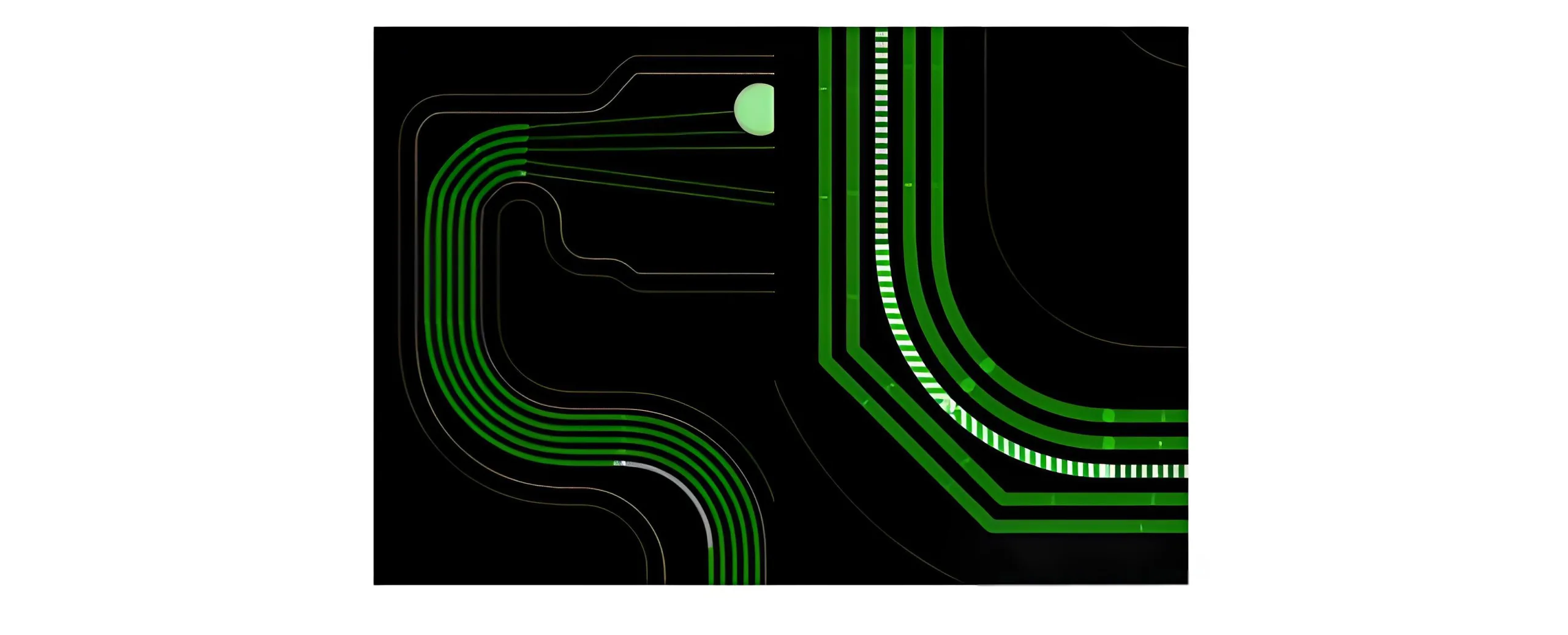
4. Принципы маршрутизации: Электро-механический баланс
4.1 Запреты зоны изгиба
-
Нет вайсов/компонентов в пределах 5 мм от изгиба
-
Шофы с прилегающими слоями. “I-Beam” стресс
4.2 Контроль импеданса
Характерная формула импеданса для высокоскоростных сигналов:
Z₀ = [87/√(эн<подставка>ведущий</подставка>+1.41)] × ln[5.98час/(0.8W+T.)]
Среди них, энведущий Диэлектрическая постоянная, H - диэлектрическая толщина, W - ширина линии, и t - толщина меди.
Дифференциальная серплентная маршрутизация (2× интервал) минимизирует перекрестные помехи.
5. Производственное сотрудничество
5.1 IPC-2581 Стандартная реализация
Unified XML -формат уменьшает ошибки связи 80%, повышение урожайности первого прохода из 65% к 92% в проектах антенны беспилотников.
5.2 Руководящие принципы DFM
-
Интернет -интервал: ≥4 млн
-
Лазерное бурение: ≥4 миль отверстий (± 1 миль точности)
-
Покрывающие отверстия: 0.1мм больше, чем прокладки
6. Будущие границы
6.1 3D растягиваемые цепи
Процесс 3D-LSC от UESTC включает в себя гибкие схемы масштаба с 5-слойным стеком, применяется в медицинских носимых устройствах.
6.2 Наноматериальные прорывы
Композиты графена/PU достигают 10<Как дела>-6</Как дела> Ω · CM удельное сопротивление с деградацией производительности < 5% после изгиба 100 тыс..
Заключение
Гибкий дизайн печатной платы требует междисциплинарных инноваций в материалах, механика, и электроника. Внедряя эти стратегии и приняв новые стандарты, такие как IPC-2581, Инженеры могут разработать гибкие цепи следующего поколения с повышенной надежностью и плотностью для передовых приложений.
