
Тихая материальная революция изменяет электронику
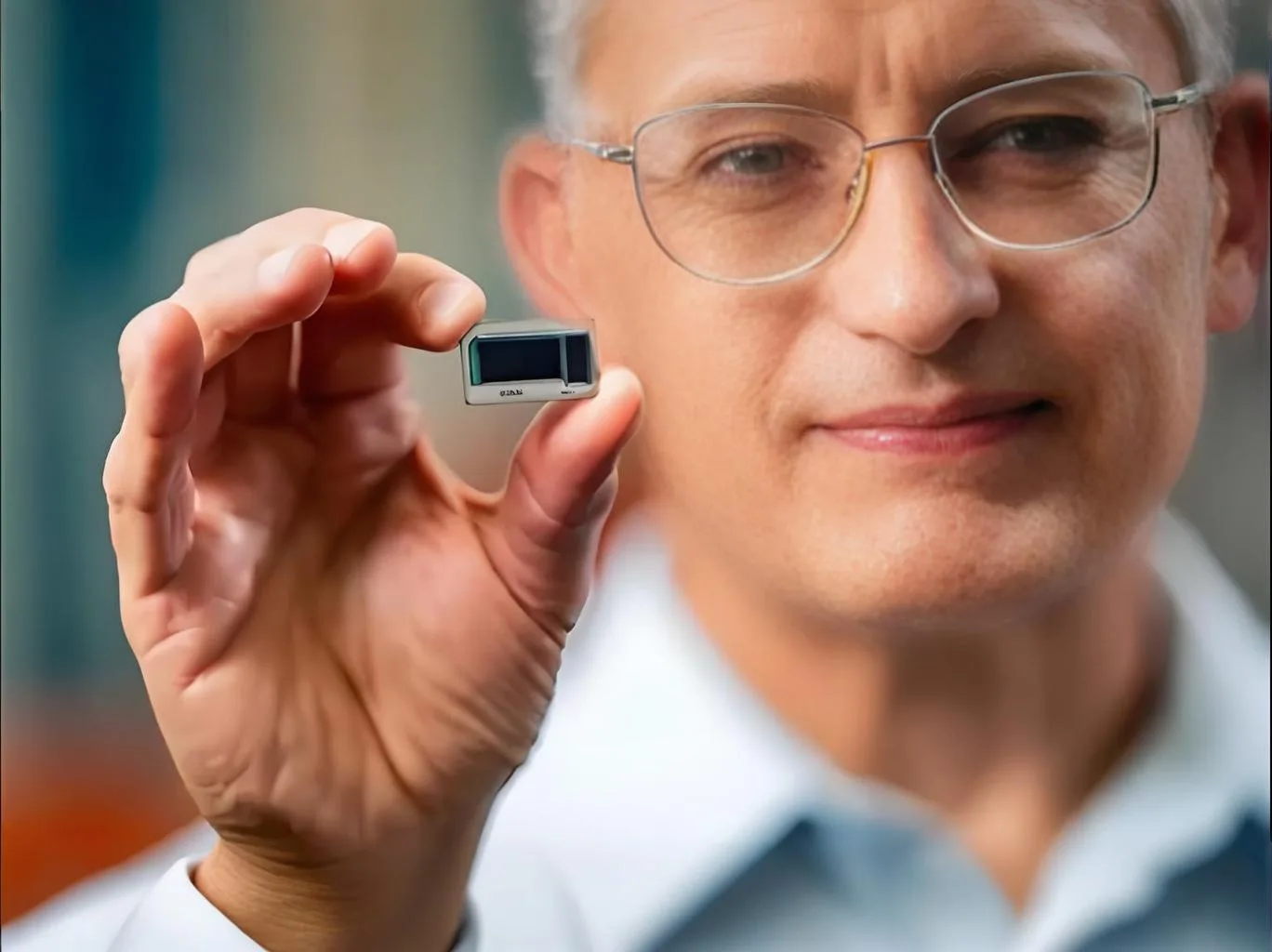
Intel's 2024 Глобальный дебют стекла подложка упаковка Технология взорвала сейсмический сдвиг в производстве полупроводников. В 2025 Suzhou TGV Industry Summit, Технические лидеры из Intel, TSMC, и Samsung согласился: “Стеклянные субстраты будут вводить полупроводниковую упаковку в прозрачную эру,’ с превышением проникновения рынка 50% в течение пяти лет.” Этот анализ исследует технологическое обоснование, Трансформация промышленной цепи, и последствия для печатная плата промышленность.
1. Техническое превосходство: Почему стеклянные субстраты переопределяют упаковку
1.1 Доминирование физической собственности
Сравнительный анализ выявляет стеклянные субстраты’ Подавляющие преимущества :
| Параметр | Органические субстраты | Кремниевые интерпозеры | Стеклянные субстраты |
|---|---|---|---|
| Диэлектрическая проницаемость | 4.2-4.8 | 11.9 | 3.9 |
| Потеря касательной | 0.02-0.04 | 0.001-0.01 | 0.0001-0.001 |
| КТР (ppm/° C.) | 16-18 | 2.6 | 3.2-7.5 (Настраиваемое) |
| Теплопроводность | 0.2-0.3 | 150 | 1.1 |
| Шероховатость поверхности | 0.5-1.0 мкм | 0.05 мкм | <0.01 мкм |
(Источник: Intel Техническая белая бумага, Корнинг материалы лаборатория)
Анализ уравнения потери сигнала
Затухание (а) определяется как:

С ε’≈3,9 и ε”≈0,001 для стеклянных субстратов, высокочастотный (100ГГц) Потери уменьшаются на 67% по сравнению с органическими субстратами (E'4.5, эн”≈0.03).
1.2 Усиление экспоненциальной плотности
GPU NVIDIA GB200 демонстрирует 50%+ Увеличение количества матриц с использованием стеклянных субстратов, достижение плотности проводки 5 мкм/5 мкм через:
-
Атомная плоскостность (<0.01мкм шероховатость)
-
Настраиваемое сопоставление CTE (3ppm/° C.)
-
Механическая стабильность (700× 700 мм панель <50мкм)
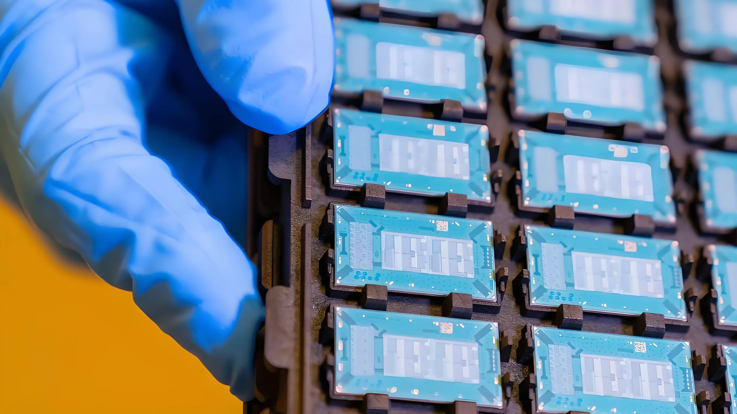
2. Процесс инноваций: Индустриализация технологии TGV
2.1 Прорывные прорывы из производства стекла-VIA
Лазерная модификация Titanrise Tech достигает 8,000 Vias/Sec при ± 5 мкм точности (3а), 160× быстрее, чем обычные методы. Ключевые шаги:
-
Пикосекундная лазерная модификация: Создает измененные зоны микронного масштаба
-
HF травление: Достигает 100:1 Соотношение сторон
-
Металлизация: ПВД распыление + гальваника (>15МПА адгезия)
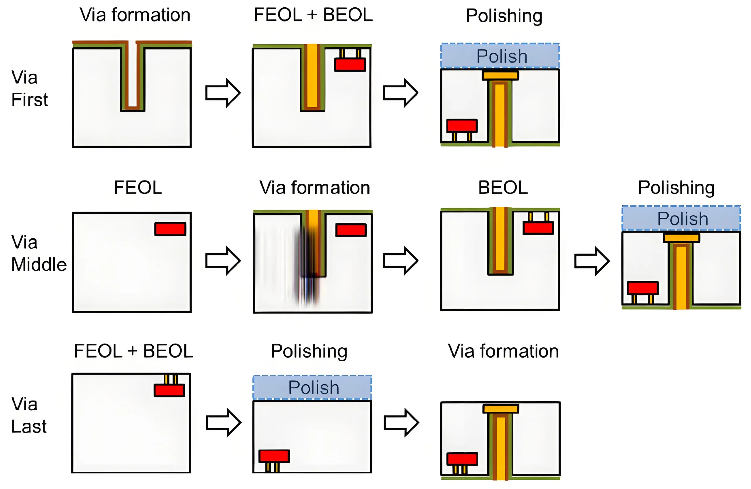
2.2 Достижения металлизации
Четыре технических маршрута решают стеклянную адгезию:
-
Без электро + Микро-чаевые (AKM Solutions)
-
Нано-аг-паста + LT спекание (Wintech Patent)
-
Плазма прививка (IME-CAS Technology)
-
Pvd Ti/со стеком (Стандарт Титана)
Среди них, УГКПБ вложил значительные средства в внедрение оборудования DEP600, который использует технологию распыления с высоким соотношением сторон, достижение 95% покрытие в 10:1 Профили отверстия, с удельным сопротивлением металла меньше, чем 2.5 μОМ · см, достижение на международном уровне.
3. Промышленная ландшафт: Глобальная конкуренция усиливается
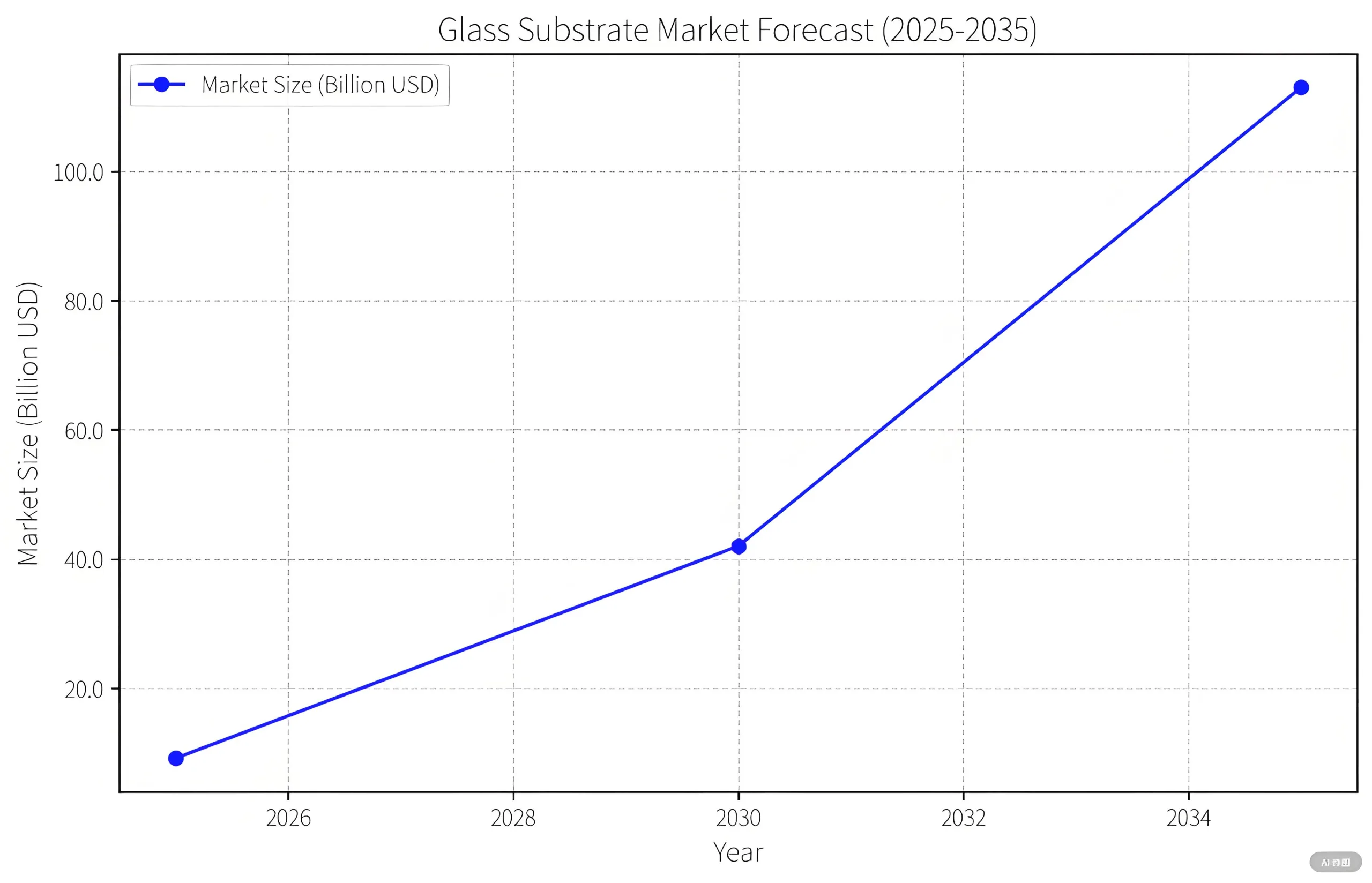
3.1 Прогнозы роста рынка
Prismark прогнозирует взрывное расширение:
-
2025: $916М (ТГВ субстраты)
-
2030: $4.2Б (Полные приложения)
-
2035: $11.3Б (Вся экосистема)
3.2 Геополитическая техническая гонка
-
США: Стандарты Intel + Доминирование по подаче корнинг
-
Корея: Samsung's “Стеклянный альянс” + 9-слойные стеки SKC
-
Китай: Wintech/AKM Mass Production + Jfe 2026 локализация
4. Проблемы & Решения: Коммерциализация препятствий
4.1 Пути снижения затрат
Текущий 3-5 × стоимость премия против традиционных субстратов будет падать через:
-
85% большая панель (>2м²) Использование
-
90% Снижение затрат на бурение на лазер
-
Улучшение урожайности металлизации (60%→ 92%)
4.2 Сертификация надежности
Требуются новые стандарты:
-
Термический велосипед (-55° C - 2550 ° C., 1,000 цикл)
-
EM Lifetime (Mttf >10⁷ часы @ jep154)
-
Высокочастотная стабильность (<0.5DB/CM @100 ГГц)
5. Последствия отрасли ПХБ: Угроза против возможности
5.1 Нарушение рынка
-
30% HDI/субстрат риск замены
-
Гибридный (стекло+смола) Возможности субстрата
5.2 Технологическая синергия
-
Пикосекундное лазерное бурение
-
ПВД-усиление ИЧР Трочие точности
-
Оптическая проверка <0.1Резолюция мкм
Заключение: Прозрачные субстраты, Непрозрачное будущее
Китай теперь возглавляет критические секторы TGV (оборудование, тестирование, материалы). Как отмечает Pat Gelsinger из Intel: “Материальные инновации становится новым законом Мура в атомных масштабах.” Эта стеклянная революция может разблокировать вторую кривую роста полупроводника.
