
Продолжительность приподкой прокладки BGA с приподкой BGA может забрать смартфон с смартфоном в размере. “Белый экран пресс-папье” - В то время как традиционная недостаточная заполнение просто маскирует эту критическую угрозу надежности ПХБ.. Поскольку смартфоны быстро развиваются в сторону ультратонких конструкций и высокоэффективных характеристик, BGA Pad Cracking стал Дамоклами’ Меч свисает печатная плата Производство. Когда а $1,000+ мобильный телефон Сборка печатной платы становится отходом из-за микросхем или рыночных ставок доходности 30% от Плохи типа V., Мы должны спросить: Несомненно, является конечным решением?
1. BGA Pad Cracking: Невидимый убийца электроники
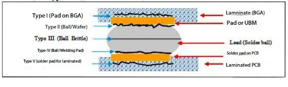
H3: 1.1 Определение неудачи & Пять типов переломов
BGA Pad Cracking относится к разделению между Чипсы IC и прокладки печатной платы под механическим/тепловым напряжением. Пять типов переломов классифицируются по местоположению:
| Тип | Расположение неудачи | Распространенность | Первичные триггеры |
|---|---|---|---|
| Тип i | Чип -субстрат слой | 12% | Упалостные тесты, механический шок |
| Тип II | BGA Pad-Sodder Interface | 18% | Термический велосипед |
| Тип III | Бесполетный паяный мяч | 25% | Удары, тепловой удар |
| Тип IV | Соединение паутины-PCB | 28% | Несоответствие профиля |
| Тип V. | Pad-Substrate разделение | 17% | Структурная деформация, деградация материала |
1.2 Стелс природа & Разрушительное воздействие
Традиционная проверка SMT обнаруживает <5% изделия из прокладки из -за:
-
Размеры микро-трещины (5-50мкм) Заткнуты в многослойных печатных платах
-
Электрическая непрерывность часто поддерживается, несмотря на переломы
-
Маскими масками, не останавливая распространение, требует разрушительного удаления во время переделки

2. Анализ основной причины в PCBA Workflow
2.1 Материальное происхождение: Кристаллическая структура медной фольги
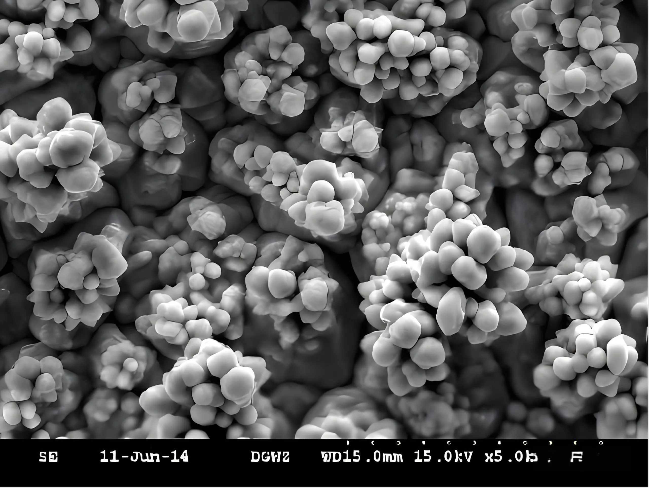
Экспериментальные данные показывают: Медная фольга со специализированной “виноградный” Узелкулярные структуры обеспечивают 18.5% более высокая адгезия, чем обычные кристаллы.
2.2 Подложка PCB Ограничения: Термический кризис FR4
Проблемы без свинца потребности в пиковых температурах 248 ° C (+33° C против традиционных процессов). Стандартные FR4 TG 130-140 ° C. причины:
-
Z-ось Cte >300 ppm/° C.
-
T288 время расслоения <3 мин (Промышленность требует >5 мин)
Критическая формула: Тепловое напряжение = E × α × ΔT
Где:
σ = тепловое напряжение (МПА), E = модуль упругости (Средний балл),
α = cte (ppm/° C.), ΔT = изменение температуры (°С)
*Субстраты с высокой CTE генерируют 1,8 × больше напряжения при ΔT = 100 ° C*
2.3 Проектирование печатных плат Ловушки: Упускается из виду механическое напряжение
Анализ 7,000 Неудачные подразделения на российских рынках показывают:
-
0.80Доски MM не удалось 3,2 × более 1,00 мм доски
-
Слоты Т-карты увеличили риск растрескивания PCBA на 47%
-
Большие компоненты в зонах BGA вызывали асимметричную тепловую деформацию
3. Критические прорывы управления процессом печатной платы
3.1 Матрица оптимизации производства печатной платы
| Процесс | Общепринятый | Оптимизированный | Улучшение |
|---|---|---|---|
| Медная фольга | Стандартные узелки | Виноподобные кристаллы | Адгезия ↑ 18,5% |
| Толщина покрытия | 18-23мкм | ≥30 мкм | Растяжение ↑ 32% |
| Поверхностная подготовка | Шлифование ремня | Микро-чашка + спрей | Потеря меди ↓ 60% |
| Открытие паяной маски | Циркуляр | Гексагональный | Поток вставки ↑ 40% |
3.2 Революция профиля
Сбой корня: Стандартный рефтоу тратит только 12S охлаждение от 190 ° C → 130 ° C, вызывая быстрое сокращение.
Решение: Продлить время задержки над TG 150%, уменьшение теплового напряжения 35%.
4. Комплексная база данных решений PCBA
4.1 Дизайн инновации
-
Геометрия прокладки: Преобразовать периферические прокладки в овальные (Длинная ось +0,1 мм)
-
Дизайн стека: Добавить локализованные слои баланса меди в BGAS
-
Правило разрешения: Запрещать большим компоненты В пределах 3 мм от зон BGA
4.2 Путь обновления материала
-
Укажите FR4 с TG ≥170 ° C
-
Управлять медной фольгой RZ (шероховатость) при 3,5-5,0 мкм
-
Принять с низким CTE (<2.5%) Системы смолы с высокой каплей
4.3 Процесс управление красными линиями
-
Медное покрытие ≥30 мкм (подтвержден)
-
OSP панели между панелями >5мм (профилактика кислотного улавливания)
-
Давление испытательного приспособления ≤7 кг/см², Жизнь булавки <500К цикл
-
150-180° C зона отбоя проживания ≥90 секунд
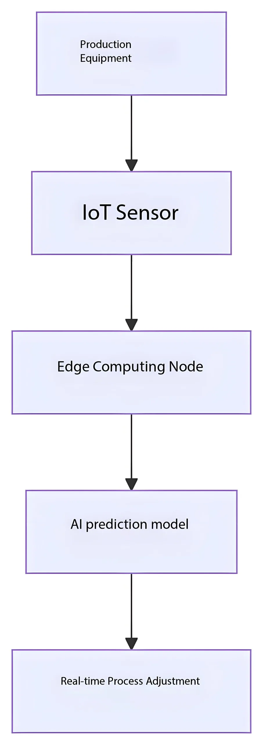
5. Будущая технологическая дорожная карта
Как HDI PCBS продвигаться к толщине 0,4 мм и BGA Pads сокращаются ниже 0,2 мм, Требуются прорывы:
-
Наномасштабное лечение меди: Магнетроно-заплестанные слои адгезии
-
CTE-адаптивные субстраты: Температурные полимерные композиты
-
ИИ мониторинг процесса: Прогноз здоровья припов в режиме реального времени
Заключение: Надежность разработана в
BGA Pad Cracking составляет Отказ надежности на уровне системы. Результаты после внедрения:
-
Повышенная скорость прохождения: 82% → 99.6%
-
Рыночная доходность: ↓ 70%
-
Снижение затрат: $1.20/Правление через ликвидацию недостаточно
*Помнить: Увеличение адгезии на падку на 0,1 кг кг.. Это превосходит уточнение процесса-оно воплощает в себе окончательное стремление к производству с нулевым дефектом.*
В микроскопической сфере припоя, Виноподобные медные кристаллы плетение наномасштабных защитных сетей, В то время как сферы без свинца выполняют точные танцы в отверстиях шестиугольной маски. Революция по надежности электроники начинается с непоколебимой приверженности каждым 0,01 мм.
