
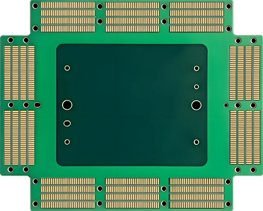
Введение в 58-слойную плату Eate Load Load
58-х слоя съел (Автоматизированное испытательное оборудование) Загрузка платы-это высокая плотность, многослойный печатная плата спроектировано для передачи точной передачи сигнала и долговечности в требованиях тестирования. Разработано с расширенными параметрами, Он обеспечивает оптимальную производительность в высокочастотных и мощных приложениях.
Ключевые спецификации
-
Слои: 58
-
Размеры: 17.2″ x 17.8″
-
Толщина: 230 мил
-
Материал: FR4 TG185
-
Минимальный размер отверстия: 5 мил
-
BGA -интервал: 0.8 мм
-
Соотношение сторон: 23.4:1
-
Расстояние для тренировки: 7 мил
-
Пофв (Нанесенный наполненным через): Да
-
Назад бурение: Нет
-
Поверхностная отделка: Eneg+Tg+только
Дизайн и структурные особенности
Критические соображения дизайна
-
Высокий уровень слоя: 58-слояная структура поддерживает сложную маршрутизацию для взаимодействия высокой плотности (ИЧР), Минимизация потери сигнала.
-
Выбор материала: FR4 TG185 обеспечивает тепловую стабильность (до 185 ° C температура перехода стекла), критическое для мощных применений.
-
Точное бурение: А 5 Мил минимальный размер отверстия и 23.4:1 Соотношение сторон, необходимо для BGA (0.8 мм шаг) Интеграция компонентов.
-
Целостность сигнала: Контролируемый импеданс и 7 Промежуточное расстояние в Mil Drill to-Copper уменьшает перекрестные помехи и электромагнитные помехи (Эми).
Уникальные структурные преимущества
-
Технология POFV: Повышается через надежность путем заполнения и покрытия вага, Улучшение тепловых и механических характеристик.
-
ENEG+TG+ENIG Surface Finish: Комбинирует электрополосное никелевое золото (Энэг) и погружение золота (СОГЛАШАТЬСЯ) Для превосходной коррозионной стойкости и припадения.
Производительность и приложения
Операционные принципы
Печатная плата облегчает точную маршрутизацию электрического сигнала через 58 слои, Использование диэлектрических свойств FR4 TG185 для поддержания целостности сигнала. POFV обеспечивает надежные соединения в среде высокого стресса, В то время как оптимизированное соотношение сторон поддерживает стабильные высокочастотные операции.
Ключевые показатели производительности
-
Тепловое сопротивление: Выдерживает температуру до 185 ° C.
-
Механическая стабильность: Высокий материал TG предотвращает расслоение при термическом велосипеде.
-
Скорость сигнала: Диэлектрический материал с низким потери.
Основные варианты использования
-
Автоматизированное испытательное оборудование (ЕЛ): Используется в системах полупроводникового тестирования для проверки ICS и микропроцессоров.
-
Аэрокосмическая и защита: Развернуто в радарных и коммуникационных системах, требующих высокой надежности.
-
Телекоммуникации: Поддерживает инфраструктуру 5G и высокоскоростную передачу данных.
-
Автомобильная электроника: Интегрируется в ADAS (Расширенные системы помощи водителю) и модули питания EV.
Производственный процесс и обеспечение качества
Производственный рабочий процесс
-
Подготовка материала: FR4 TG185 Ламинаты вырезаны до 17,2″ x 17.8″ размеры.
-
Лазерное сверление: Создает 5 Мил Микровий с 23.4:1 Соотношение сторон.
-
Покрытие и наполнение: Технология POFV применяет медное покрытие к заполненным вагам.
-
Слой стек: 58 слои выровняются и связаны под высоким давлением.
-
Поверхностная отделка: ENEG+TG+ENIG COTPATE применяется для защиты от коррозии.
-
Тестирование: Электрическая непрерывность, импеданс, и выполняются испытания на тепловые стресс.
Стандарты контроля качества
-
IPC-6012 Класс 3: Обеспечивает надежность для суровых средств.
-
Контроль импеданса: ± 10% допуск поддерживается.
Резюме преимуществ
-
Проект высокой плотности: Поддерживает сложные схемы в компактных пространствах.
-
Тепловая устойчивость: FR4 TG185 обеспечивает стабильность в экстремальных условиях.
-
Прецизионная инженерия: 5 MIL отверстия и 0,8 мм BGA -расстояние Включите миниатюрную интеграцию компонентов.
-
Универсальные приложения: От полупроводникового тестирования до 5G инфраструктуры.
Эта печатная плата сочетает в себе передовую конструкцию, Строгие стандарты производства, и надежные материалы для удовлетворения потребностей критически важной промышленности.


