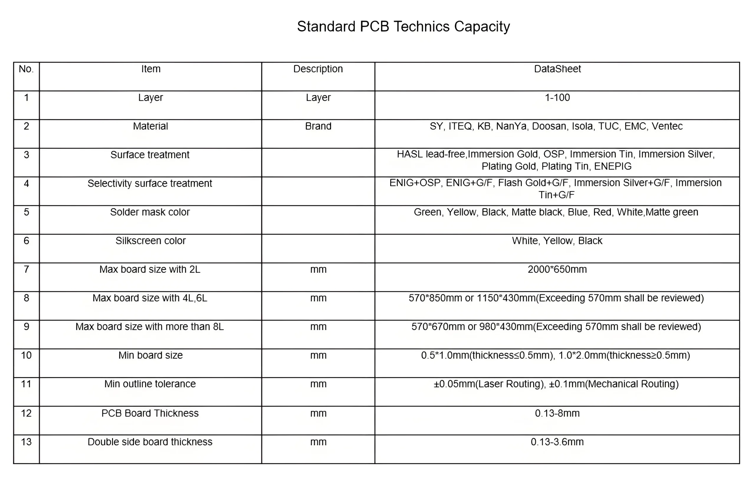
Precision Circuit Imaging & Etching Technology
UGPCB Factory demonstrates exceptional process control in circuit patterning and etching. For standard PCB production, we consistently achieve:
- Laser Direct Imaging (LDI) replacing traditional photolithography masks, enabling digital file-based exposure with ±5μm alignment accuracy
- Alkaline etching process ensuring clean line edges with ±15% line width control (industry-leading tolerance)
- Expertise in handling various copper thicknesses (1oz-6oz) with minimized side-etching
High-Precision Drilling & Hole Metallization
Our drilling capabilities cover:
- Mechanisches Bohren for 0.4mm-3.0mm boards with ±0.025mm hole size tolerance
- Laserbohrung down to 0.1mm microvias
- Hole metallization Erreichen >20μm uniform copper plating through advanced chemical deposition and electroplating
- Special processes for 8:1 Zu 10:1 aspect ratio requirements
Multilayer Lamination & Interlayer Alignment
- Up to 100-layer PCB fabrication using FR-4 Grade A materials
- Precision lamination with ±15um layer-to-layer alignment
- Temperature/pressure/time-controlled processes preventing delamination
- Options for high-Tg materials, high-speed laminates, and heavy copper up to 1000μm
Lötmaske & Surface Finish Options
- Solder mask colors: Green/Blue/Red/Black with 0.08mm minimum solder bridge
- Oberflächenbewegungen:
- Bluten (Heißluftlötes Leveling)
- ZUSTIMMEN (Elektrololes Nickel -Eintauchgold)
- Immersion Tin/Silver
- OSP (Bio -Lötlichkeitsschutz)
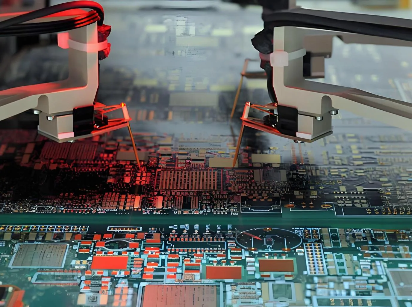
Comprehensive QC & Testing Systems
- AOI -Inspektion: High-resolution defect detection for line/space, Pads, shorts/opens
- Impedanzkontrolle: ±10% tolerance for high-speed/RF applications
- Elektrische Tests: Fliegende Sonde & fixture-based continuity verification
- Reliability Testing: Thermoschock, humidity resistance, flexural testing
Process Capability & Stabilität
- CPK >1.33 (4A) across critical processes, reaching 1.67 (5A) in key areas
- Line width control within ±15% (vs industry 20% Standard)
- Statistical process control (SPC) ensuring consistent production quality
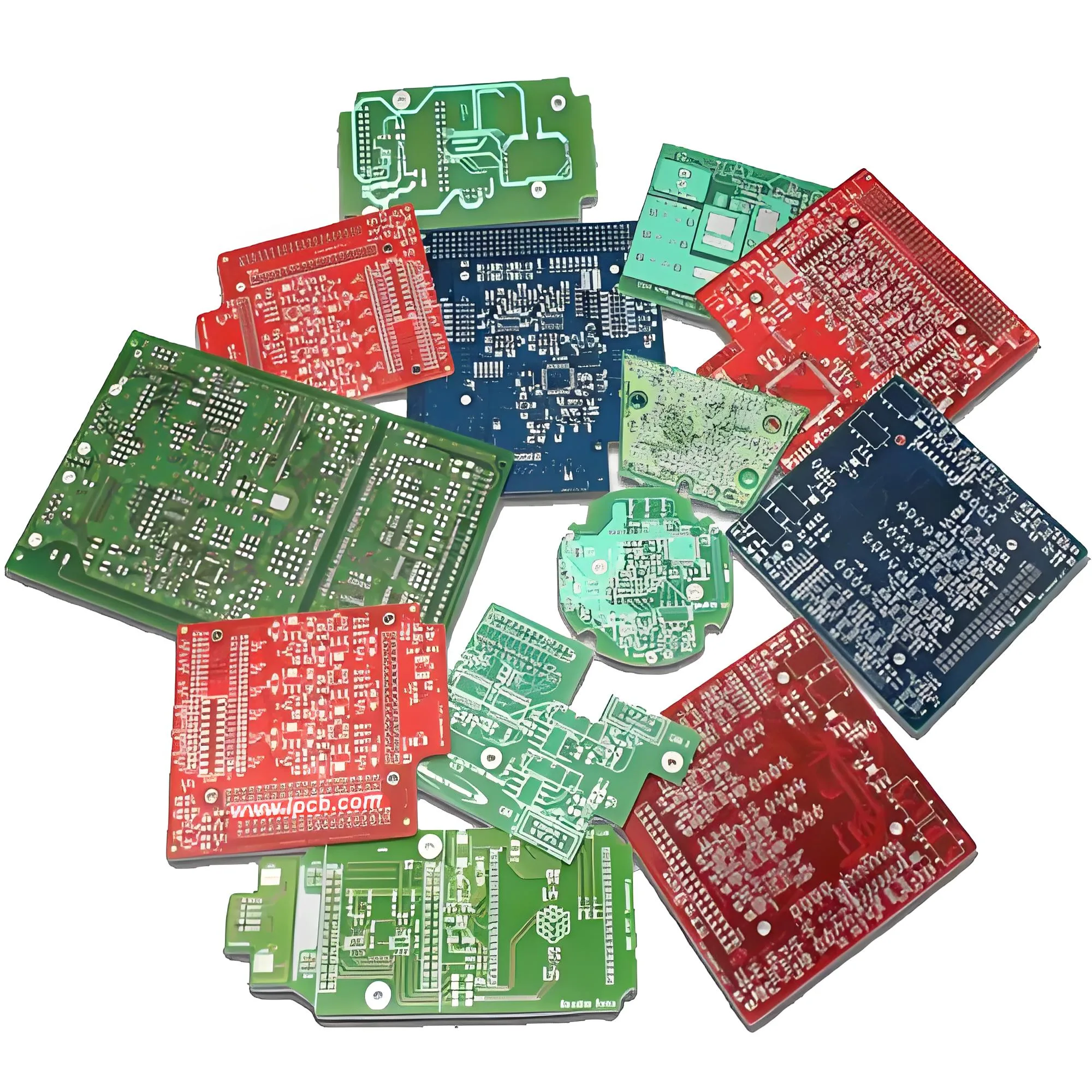
PCBA One-Stop Services
- SMT Assembly: 01005 component handling with ±0.03mm placement accuracy
- Erweiterte Verpackung: BGA/Micro BGA/PoP support with X-ray inspection
- DFM Support: Impedance calculation, Stapeldesign, manufacturability analysis
Branchenanwendungen & Kontakt
Serving consumer electronics, Industrielle Steuerungen, Telekommunikation, medizinische Geräte, and automotive sectors with tailored PCB solutions. Visit our website for process capability reports and free DFM consultation.
WeChat
Scannen Sie den QR-Code mit WeChat