
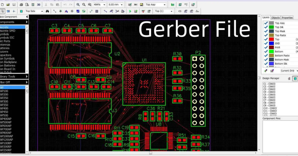
Einführung: Gerber -Dateien - Die DNA der PCB -Herstellung
In Hochgeschwindigkeits-PCB-Design, Gerber -Dateien übertrieben über 90% von Fertigungsdaten. Gemäß den IPC-2581-Standards, 85% von global PCB -Hersteller Verlassen Sie sich auf Gerber als primäre Produktionsdokumentation. Als die “Industrial Blueprint” der Elektronik, Gerber -Dateien beschreiben die physikalische Struktur einer Leiterplatte genau durch geschichtete Codierung. Diese Anleitung dekodiert die technische Bedeutung jeder Schicht, um Ihnen zu helfen, zu meistern Leiterplattenfertigung.
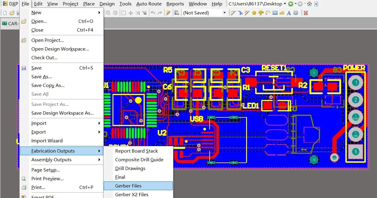
Abschnitt 1: Vervollständigen Sie den Workflow von Gerber -Dateien Exportieren
1.1 Überprüfung vor dem Export
-
DRC -Validierung: Stellen Sie die Einhaltung von IPC-2221-Standards sicher (Min. Trace/Space = 0,1 mm @ 6-Layer Leiterplatten)
-
Stackup -Bestätigung: Impedanzkontrolle muss erfüllen:

Wo H = dielektrische Dicke, W = Spurbreite, T = Kupferdicke (1 oz = 35 µm).
1.2 Exportmodusvergleich
| Verfahren | Anwendungsfall | Datei Vollständigkeit |
|---|---|---|
| Ein-Klick-Export | Standard 4-6 Layer -PCBs | 95% |
| Benutzerdefinierte Konfiguration | HDI-Leiterplatten / Blind/begrabene Vias | 100% |
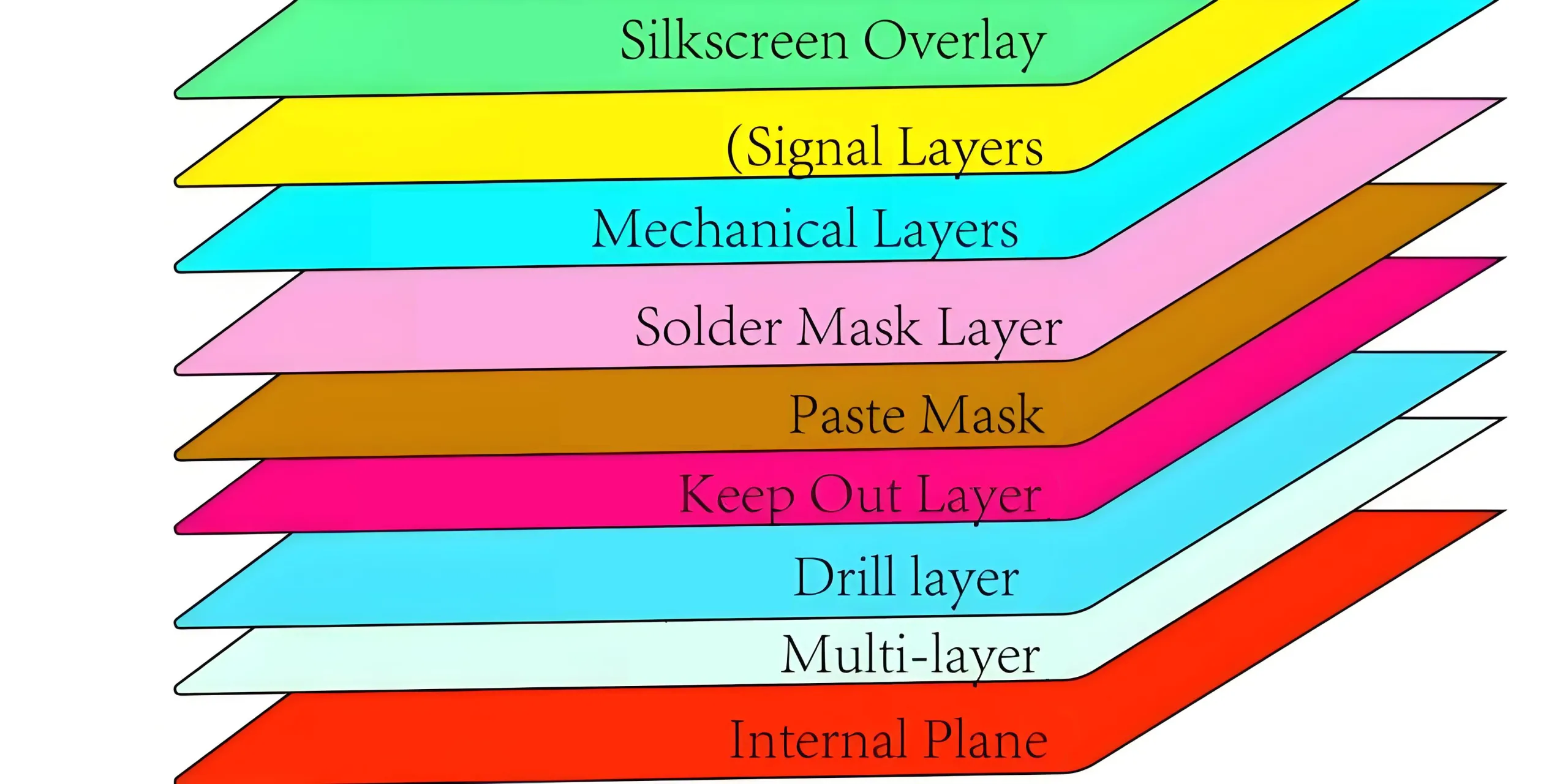
Abschnitt 2: Gerber -Schicht -Struktur Deep Dive
2.1 Leitfähige Schichten erklärt
Kupferschichten:
-
Obere/untere Schicht: Oberflächenrouting (Typ. 1 Oz Kupfer)
-
Innere Schichten: 6-Layer PCB Stackup: Top-Gnd-Signal-Signal-Signal-Bottom
Bohrschichten:
2.2 Prozessunterstützende Schichten
Lötmaskenschicht:
-
Negative Bildausgabe (Enthält Kupferöffnungen)
-
Min. Freigabe: 0.07mm (Verhindert Lötmaskenüberbrückungsfehler)
Maskenschicht einfügen:
-
Schablone Apertur = Padgröße × 90%
-
QFN-Pakete erfordern Cross-Bridge-Anti-Solder-Perlen-Design
Seidenschicht:
-
Texthöhe ≥0,8 mm, Linienbreite ≥0,15 mm
-
Die untere Schicht Siebbildschirm erfordert Spiegelung
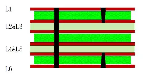
Abschnitt 3: Gerber Funktionen in mehrschichtigen PCBs
3.1 Schichtzahl vs. Gerber -Dateien
| PCB -Schichten | Gerber -Dateien | Besondere Anforderungen |
|---|---|---|
| 1-2 | 8-10 | Standard-Durchlöcher |
| 4-6 | 15-20 | Impedanzkontrolle + Vippo |
| 8+ | 25+ | Blind Vias + Hybridstapel |
3.2 Erweiterte Prozessumsetzung
Vippo (VIC-in-Pad):
-
Lochdurchmesser ≤ 0,15 mm, Padgröße ≥0,3 mm
-
Etikett als “μvia” in Bohrerschichten
Stufen -Slot -Design:
-
Mechanicallayer Annotation:
SLOT:3.0x1.2mm @ Layer2-4
Abschnitt 4: DFM -Regeln, die von Gerber -Daten angetrieben werden
4.1 Herstellbarkeitsprüfungen
4.2 Hochgeschwindigkeits-Designmarker
-
Differentialpaare:
IMPEDANCE:100Ω±10% -
RF -Spuren:
NO_SOLDERMASK(Reduziert die DK -Variation)
Abschnitt 5: Vom Layout -Ingenieur zum PCB -Architekten
Echte PCBA -Design -Experten Master:
5.1 Signalintegrität (UND)
-
Verzögerungskontrolle: ΔL ≤ 0,05√ε_R (PS/Zoll)
-
Übersprechprävention: 3W Regel (Abstand ≥ 3 × Spurbreite)
5.2 Kraftintegrität (PI)
-
Ziel Impedanz:

-
Entkoppelung des Kondensatorlayouts: Radiale Platzierung durch Kapazität
5.3 Thermalmanagement
-
Kupferstromkapazität:
I = 0,048 · ΔT0.44 Märatura0.725
(ΔT = Temperaturanstieg, A = Querschnitt)
Abschluss: Die technische Philosophie von Gerber -Dateien
Beim Exportieren von Gerber -Daten, erinnern: Diese “kalt” Schichten repräsentieren Präzisionsdialoge zwischen Elektronik und Materialwissenschaft. Von 0,05 mm Laserbohrern bis 10 μm Lötmasken -Toleranzen, Jede Gerber -Schicht erzählt die technische Philosophie der Signalisolation und leitenden Wege.
Branchendaten zeigen: Die Verwendung von Gerber+ODB ++ Dual-File-Lieferung erhöht den Erstpassertrag von Erstpass durch 40%. In der 5G/AI -Ära, Mastering Gerber -Semantik bedeutet, den Kern der intelligenten Hardwareherstellung zu steuern.


Sie lassen es tatsächlich so einfach zusammen mit Ihrer Präsentation erscheinen, aber ich finde, dass dieses Thema wirklich eine Sache ist, von der ich glaube, dass.
Es scheint für mich zu komplex und sehr umfangreich.
Ich freue mich auf Ihre nachfolgende Veröffentlichung, Ich werde versuchen, das Verständnis zu erlangen!
Ich habe es so sehr geliebt, wie Sie hier durchgeführt werden werden.
Die Skizze ist attraktiv, Ihr verfasstes Thema stilvoll.
dennoch, Ihr Befehl hat sich gegen die Ungeduld bekommen, dass Sie die folgenden Liefern liefern möchten.
Unbewusst kommt zweifelsohne ehemal mehr, da genau das gleiche fast sehr oft im Fall ist
Sie schützen diesen Anstieg.