
UGPCB 18-Lagen-Serverplatine: Entwickelt für Hochleistungsrechnen & Rechenzentren
Im Zeitalter von Rechenzentren und Cloud Computing, Serverstabilität und -leistung sind für den digitalen Geschäftsbetrieb von entscheidender Bedeutung. Als grundlegender Hardwareträger, das präzise Design und die außergewöhnliche Qualität von Server Leiterplatten (Leiterplatten) stehen im Vordergrund. Nutzen Sie umfassende Branchenkenntnisse und modernste Technologie, UGPCB sorgt für Höchstleistung, Hochzuverlässige 18-Lagen-Server-PCBs, um die anspruchsvollsten Anforderungen von Rechenzentrumsanwendungen der nächsten Generation zu erfüllen.

Produktübersicht & Definition
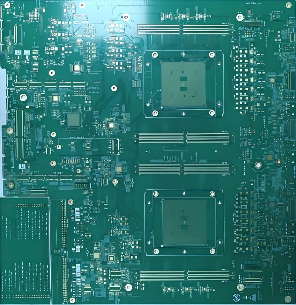
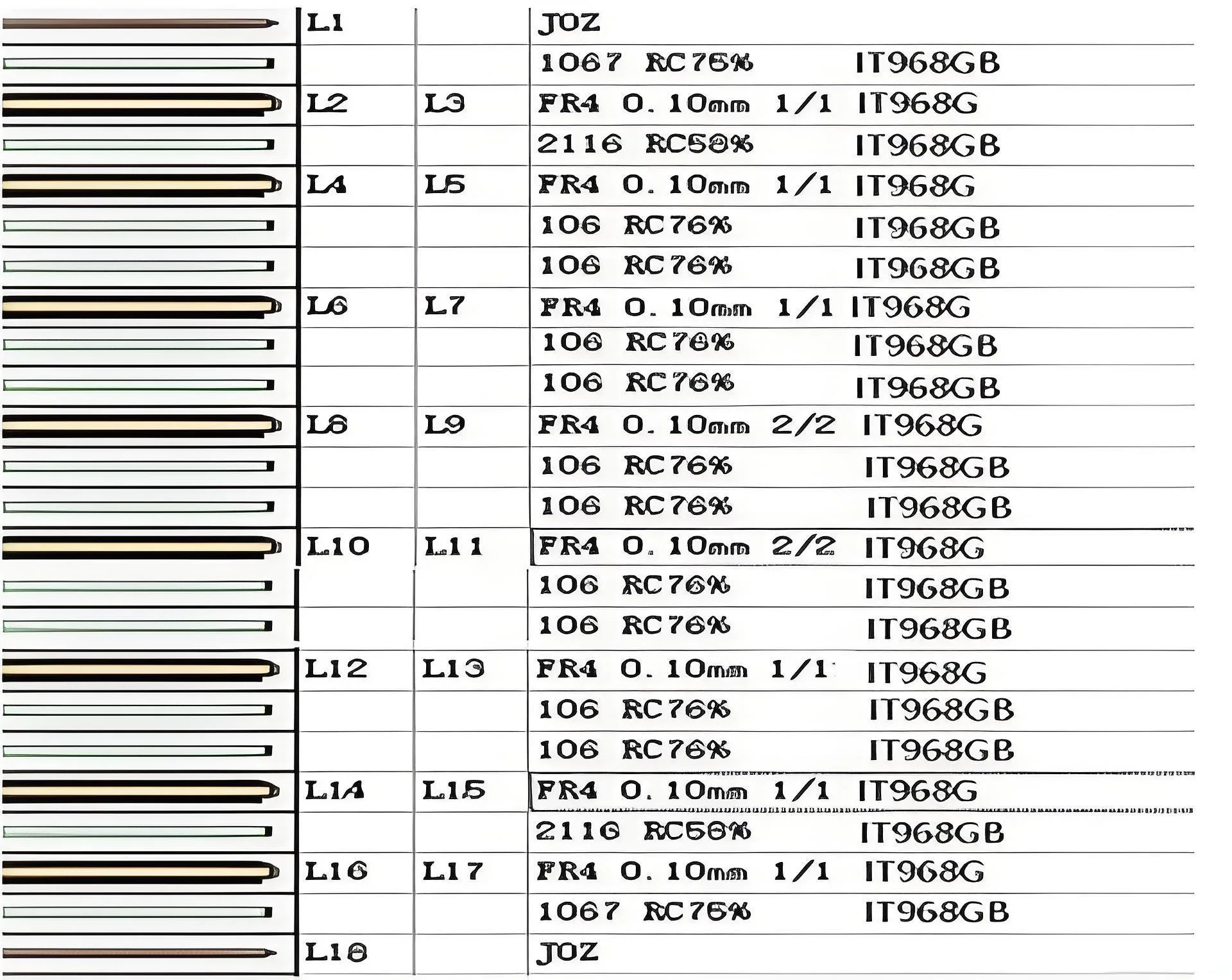
Eine Serverplatine ist die Kernkomponente von Server-Motherboards, Speicher-Backplanes, und verschiedene funktionale Tochterkarten. Es beherbergt kritische Komponenten wie CPUs, Erinnerung, und Chipsätze, Erleichterung der Hochgeschwindigkeits-Signalübertragung, Stromverteilung, und Systemvernetzung. Speziell für Hochleistungs-Anwendungsserver entwickelt, Dieses UGPCB-Produkt nutzt eine 18-lagige Mehrschichtstruktur und eine verbesserte Plattendicke von 2,4 mm ±10 %., dient als robuste Hardware-Grundlage für die Verarbeitung riesiger Datensätze und unterstützt Hochgeschwindigkeitsberechnungen.
Kerndesign-Highlights & Technische Analyse
Zur Adressierung von Serverplattformen’ extreme Anforderungen an die Signalintegrität, Machtintegrität, und thermisches Management, Dieses Produkt integriert mehrere Schlüsseltechnologien:
-
Erweitertes Stapeln & Materialien:
-
Laminieren: Nutzt die Hochgeschwindigkeitstechnologie ITEQ IT968G, verlustarmes Material. Sein hoher Tg (Glasübergangstemperatur) gewährleistet Dimensionsstabilität und konstante elektrische Leistung bei längerem Serverbetrieb bei hohen Temperaturen, Signalübertragungsverluste werden effektiv reduziert.
-
Schichten & Kupfergewicht: Ein komplexer 18-Lagen-Aufbau mit einem sorgfältig entwickelten Hybrid-Kupfer-Gewichtsschema (Mit 2 Unzen dicker Kupferfolie auf ausgewählten Innenschichten). Dies optimiert die Strombelastbarkeit und die thermische Leistung von Powerplanes und ermöglicht gleichzeitig eine feine Leitungsführung auf Hochgeschwindigkeits-Signalschichten.
-
-
Präzises Routing & Zusammenschaltung:
-
Linienfähigkeit: Erreicht eine ultrafeine Linienbreite/Abstand von 0,1 mm/0,1 mm, Erfüllt die Fan-Out- und Verbindungsanforderungen für BGA-Gehäuse mit hoher Dichte (z.B., CPU, GPU, FPGA).
-
Microvia -Technologie: Unterstützt einen minimalen mechanischen Bohrerdurchmesser von 0,20 mm, Verbesserung der Routingdichte und Raumausnutzung.
-
-
Schlüsseltechnologien für die Signalintegrität:
-
Hinterbohren: Für schnelle Differenzsignale (z.B., PCIE, SAS, Ethernet), Durch den Hinterbohrprozess werden ungenutzte Kupferstummel aus Durchgangslöchern entfernt, Dadurch wird die Signalreflexion und -dämpfung deutlich reduziert. Dies ist ein Kernprozess zur Sicherstellung der Signalqualität Hochgeschwindigkeits-PCBs.
-
RTF-Kupferfolie: Verwendet umgekehrt behandelte Folie, was für eine glattere Kupferoberfläche sorgt. Dadurch wird der Verlust des Skin-Effekts bei Hochfrequenzsignalen effektiv reduziert, Verbesserung der Signalübertragungseffizienz.
-
-
Zuverlässige Oberflächenbeschaffenheit:
-
Elektrololes Nickel -Eintauchgold (ZUSTIMMEN) wird als abschließende Oberflächenbehandlung aufgetragen. ENIG bietet eine ebene Oberfläche, ausgezeichnete Lötbarkeit, eine zuverlässige Kontaktschnittstelle, und langfristige Oxidationsbeständigkeit, Dadurch ist es ideal zum dichten Löten geeignet, Feinton Komponenten auf Serverplatinen.
-
Produktmerkmale & Vorteile
-
Außergewöhnliche elektrische Leistung: Hochgeschwindigkeits-IT968G-Laminat kombiniert mit Hinterbohren und RTF-Folie sorgt für geringe Verluste, Übertragung hochfrequenter Signale mit geringer Latenz, Dies macht es zu einer idealen Wahl für Hochfrequenz-Leiterplatten Und Hochgeschwindigkeits-PCBs.
-
Überlegene Krafthandhabung & Thermalmanagement: 2Unzen Kupfer in der Innenschicht und das 2,4-mm-Platinendesign verbessern die Strombelastbarkeit, Gesamtstruktursteifigkeit, und Wärmeleitfähigkeit.
-
Hohe Dichte & Zuverlässigkeit: Der 18-Lagen-Routingraum gepaart mit einer Linienbreite/-abstand von 0,1/0,1 mm unterstützt die komplexesten Designs. Eine strenge Prozesskontrolle und Materialien mit hoher Tg gewährleisten eine langfristige Zuverlässigkeit 24/7 unterbrechungsfreien Betrieb.
-
End-to-End-Service-Support: UGPCB bietet nicht nur Spitzenklasse Leiterplattenherstellung sondern auch eine Komplettlösung von der Designprüfung bis zur Produktion, Beschleunigen Sie Ihre Markteinführungszeit.
Überblick über den Produktionsprozess
Bei unserer Fertigung gelten strenge Vorgaben IPC -Standards und ein Qualitätsmanagementsystem:
Technische Überprüfung → Materialvorbereitung → Bildgebung der inneren Schicht → Laminierung → Bohren & Hinterbohren → Lochmetallisierung → Bildgebung der Außenschicht → Plattieren (für Hybridkupfergewicht) → Auftragen einer Lötmaske (Vor-EINS) → ENIG → Routing / Profilierung → Elektrischer Test & Endinspektion
https://via.placeholder.com/800×450.png?text=18-Schicht+PCB+Querschnitt
Alt-Text: Querschnittsansicht einer 18-lagigen Serverplatine, mit präziser Laminierung und hinterbohrten Via-Strukturen für eine Hochgeschwindigkeits-Signalübertragung.
Anwendungen & Einstufung
Diese Hochleistungs-Leiterplatte wird häufig verwendet:
-
Unternehmen & Cloud-Server-Motherboards
-
KI-Computing-Beschleunigungskarten für Rechenzentren
-
Hochleistungsspeicherserver & Backplanes
-
Netzwerk-Switch & Kernplatinen für Kommunikationsgeräte
Technische Klassifizierung:
-
Für Schichtzahl: Hoch Mehrschichtige Leiterplatte (18 Schichten)
-
Nach Technologie: Hochgeschwindigkeits-/Hochfrequenz-Leiterplatte, Hinterbohrte Leiterplatte, Schwere Kupferplatine
-
Durch Anwendung: Server-/Rechenzentrumsplatine
-
Nach Oberflächenbeschaffenheit: ZUSTIMMEN (Elektrololes Nickel -Eintauchgold) Leiterplatte
Wählen Sie UGPCB, und Sie entscheiden sich für mehr als nur eine hochwertige Serverplatine; Sie gewinnen einen vertrauenswürdigen Partner in der modernen Leiterplattenfertigung. Wir widmen uns der Umsetzung komplexer technischer Details in verlässliche Vorteile für Ihre Produkte, Stärkung Ihrer Rechenzentrumslösungen der nächsten Generation.
Kontaktieren Sie noch heute unser Expertenteam für ein individuelles Angebot für eine Leiterplattenlösung und technische Beratung!


