Materialzusammensetzung von Leiterplatten auf Kupferbasis
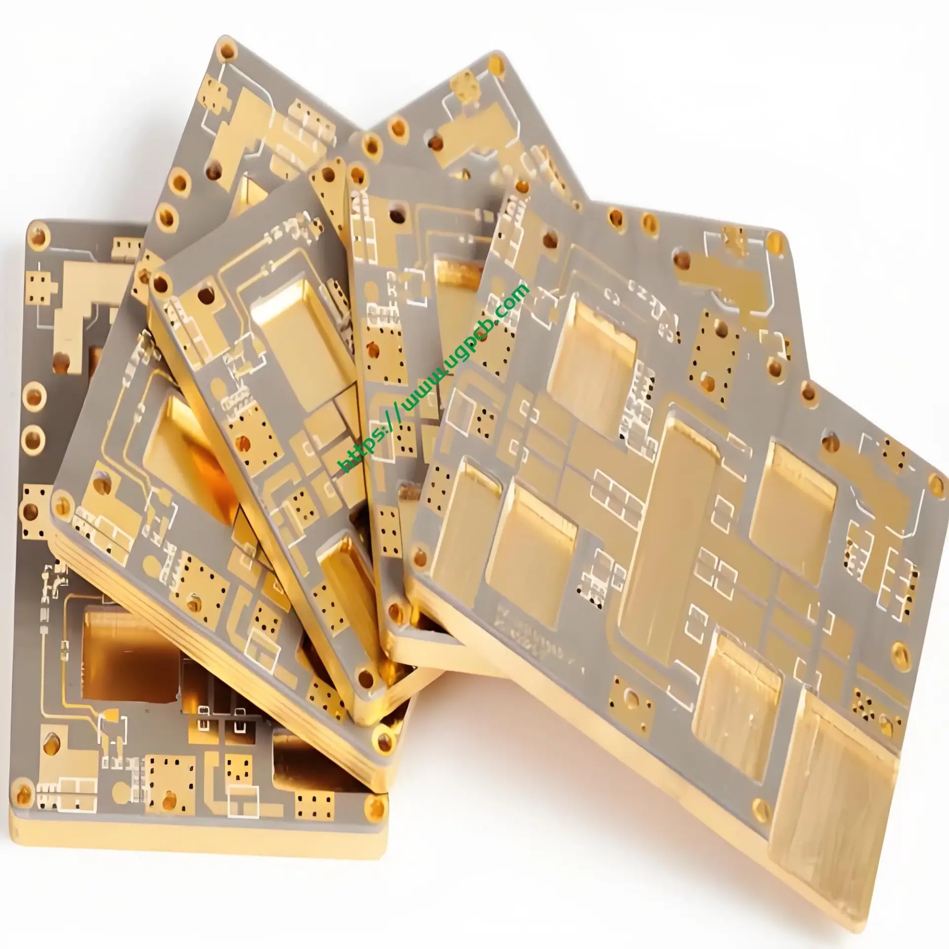
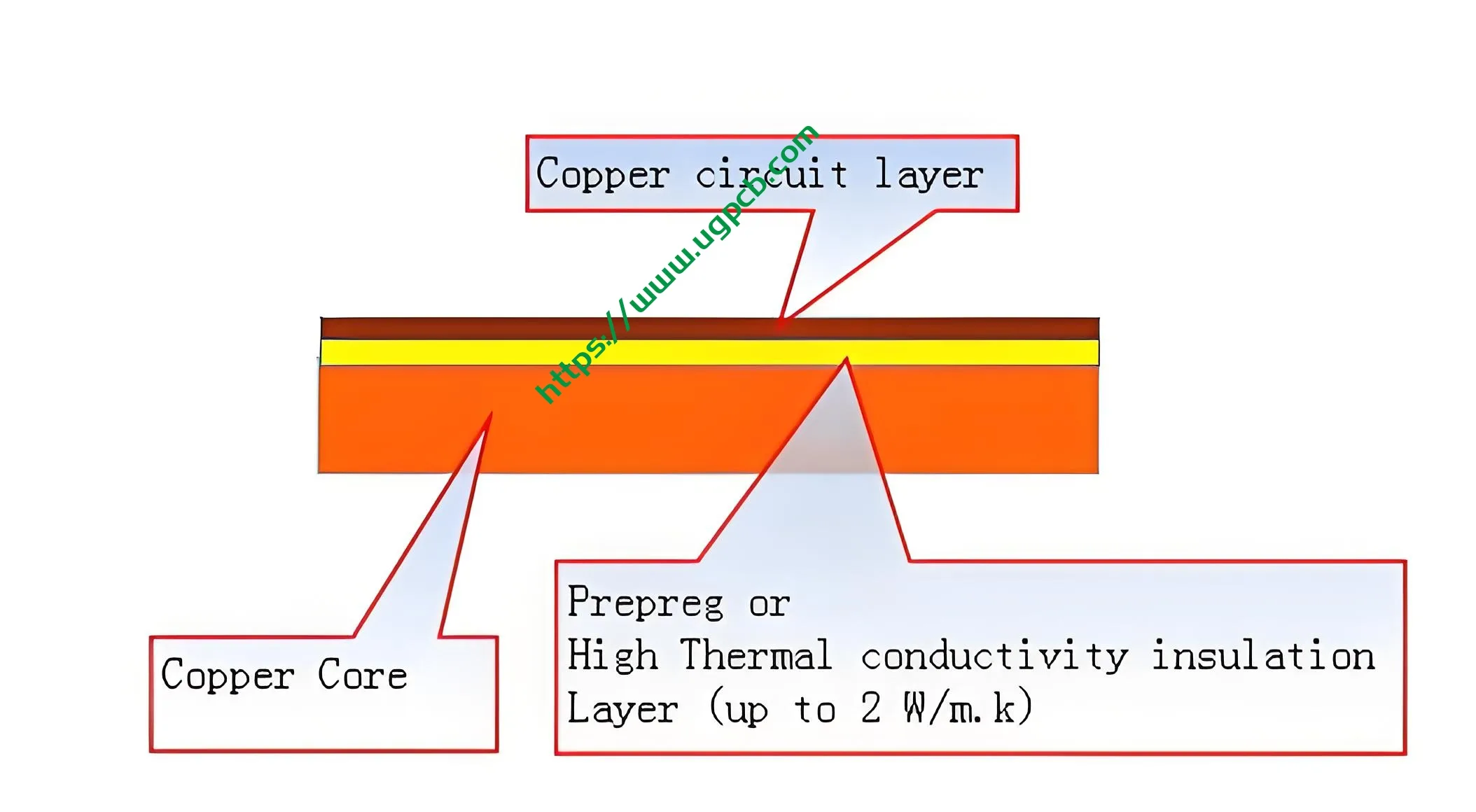
Die kupferbasierte Leiterplatte (Leiterplatte) besteht hauptsächlich aus einer Kupferbasis, das eine hervorragende Leitfähigkeit und thermische Stabilität bietet. Dieses Modell verfügt über ein einschichtiges Design, Dadurch eignet es sich für eine Reihe von Anwendungen, die effiziente elektrische Leitungen erfordern.
Leistungsfähigkeit
Mit einer fertigen Dicke von 4,0 mm und einer Kupferdicke von 3 Unzen, Das Leiterplatte ist robust und hält hohen Strömen und Temperaturen stand. Die Kupferbasis sorgt für eine hervorragende Wärmeableitung, entscheidend für die Aufrechterhaltung der Leistung in anspruchsvollen Umgebungen.
Besondere Merkmale
Erhältlich in Grün oder Weiß, Diese Platine zeichnet sich durch ihren Osp aus (Bio -Lötlichkeitsschutz) Oberflächenbehandlung, Dies schützt die Kupferschaltung vor dem Anlaufen und gewährleistet eine zuverlässige Lötung. Zusätzlich, Es verfügt über einen speziellen Prozess, der als Stufenloch-PCB bekannt ist, Ermöglicht eine mehrstufige Verbindung, ideal für komplexe Schaltungsentwürfe.
Produktionsworkflow
Die Herstellung dieser kupferbasierten Leiterplatte beginnt mit der Vorbereitung des Kupfergrundmaterials. Nächste, Die Schaltkreise werden mithilfe fortschrittlicher fotolithografischer Techniken auf die Kupferschicht geätzt. Nach dem Ätzen, Die OSP-Behandlung wird angewendet, um die Lötbarkeit des Kupfers zu erhalten. Anschließend wird die Leiterplatte auf Qualität geprüft und es werden Stufenlöcher gebohrt, ein Prozess, der vertikale elektrische Verbindungen über verschiedene Schichten hinweg ermöglicht. Endlich, Die Leiterplatte wird zugeschnitten und für den Versand vorbereitet.

Anwendungsszenarien
Aufgrund seiner hohen Leistung und Zuverlässigkeit, die Kupferbasis Leiterplatte ist ideal für High-End-Kommunikationsstromversorgungsanwendungen. Es eignet sich besonders für den Einsatz in Systemen, die eine hohe Stromverarbeitung erfordern, Robustes Wärmemanagement, und komplizierte Schaltungsdesigns. Seine Fähigkeit, Stufenlochverbindungen zu unterstützen, macht es zu einer ausgezeichneten Wahl für mehrschichtige und komplexe Leiterplatten in Telekommunikations- und Stromversorgungseinheiten.