

1. Produktübersicht
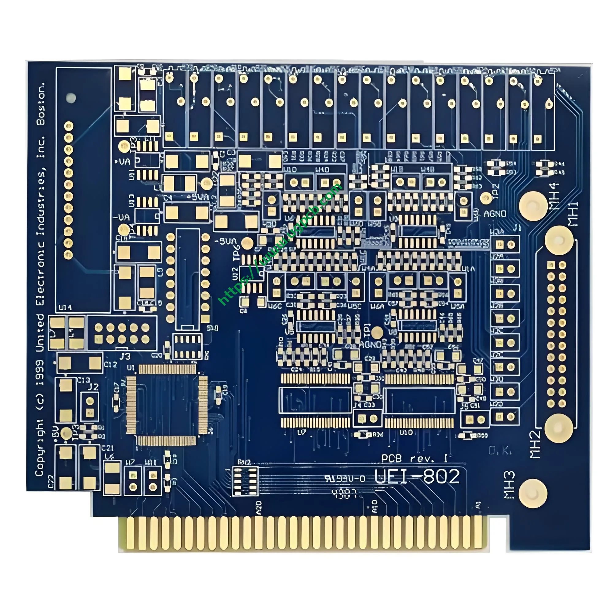
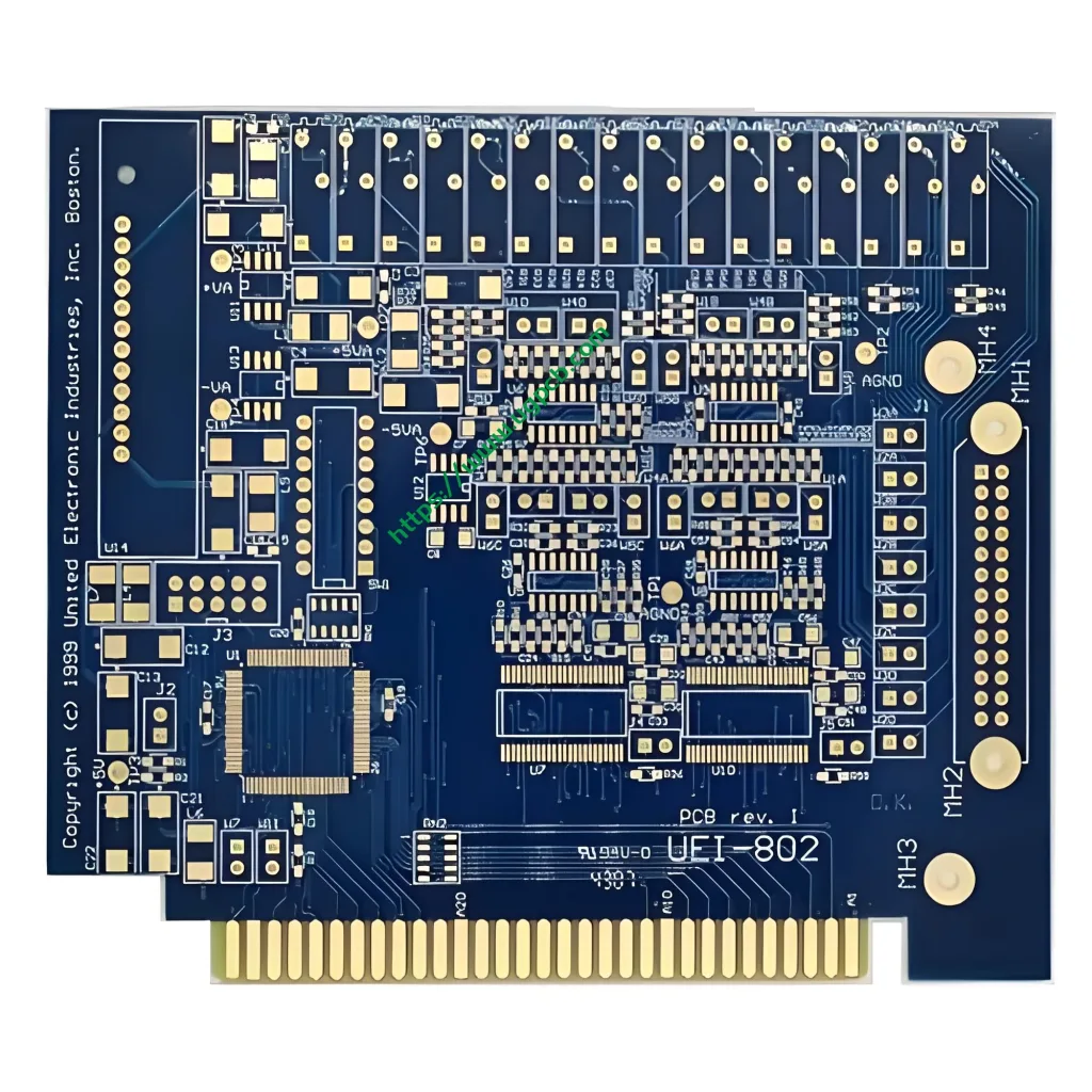
Ein doppelseitiger Goldfinger Leiterplatte (Leiterplatte) verfügt über vergoldete Kontakte – allgemein „Goldfinger“ genannt – die entlang der Platinenkante angeordnet sind. Diese Kontakte bilden beim Einstecken in einen passenden Steckverbinder einen steckbaren elektrischen Pfad, B. ein Kartensteckplatz oder ein Sockel. Alle Signale und der Strom fließen über diese fingerförmigen Anschlüsse.
Die doppelseitige Goldfinger-Leiterplatte von UGPCB verwendet ein FR4-Substrat mit einem 2-Schicht-Design. Die Plattenstärke beträgt 1.6 mm, und sowohl die innere als auch die äußere Schicht haben 1 Oz Kupfer. Der Mindestdurchmesser der gebohrten Durchkontaktierung beträgt 0.3 mm, und die Leiterbahnbreite und der Abstand sind beides 0.15 mm. Die Oberflächenveredelung ist Immersionsgold (ZUSTIMMEN) über die gesamte Tafel, mit zusätzlichem galvanischem Hartgold, das selektiv auf die Goldfingerbereiche aufgetragen wird. Dieses Produkt bietet die Routing-Flexibilität einer doppelseitigen Platine zusammen mit der bewährten Zuverlässigkeit von Goldfingerverbindungen. Es bedient eine breite Palette elektronischer Systeme, die Board-to-Board-Plug-in-Schnittstellen erfordern.
2. Produktklassifizierung und -positionierung
Gemäß IPC‑6012 (die Qualifikations- und Leistungsspezifikation für starre Leiterplatten), Dieses Produkt fällt in die folgenden Kategorien:
| Klassifizierungsdimension | Kategorie |
|---|---|
| Durch Struktur | Doppelseitige Leiterplatte – Leiterbahnen auf beiden Seiten |
| Nach Verbindungsmethode | Mit durchkontaktierten Löchern (PTH) |
| Nach IPC-6012-Leistungsklasse | Klasse 2 (dedizierter Service für elektronische Produkte) – für die meisten Goldfingeranwendungen geeignet |
| Nach Substratmaterial | FR4-Hartlaminat (Klasse S1141) |
| Nach Oberflächenbeschaffenheit | ZUSTIMMEN (Chemisches Nickel / Eintauchen Gold) + selektiv galvanisiertes Hartgold auf Goldfingern |
| Nach Funktion | Platine mit Goldfinger / Randverbinderplatine |
Dieses Produkt ist als positioniertSteckverbindung mittlerer bis hoher Zuverlässigkeit Lösung. Es kombiniert die Designfreiheit der doppelseitigen Verlegung mit der Signalintegrität von Goldfinger-Randsteckverbindern.
3. Wichtige technische Parameter
3.1 Substrat: FR4 + S1141 Laminat
FR4 ist das am häufigsten verwendete starre Substrat in der Leiterplattenindustrie. Es besteht aus glasfaserverstärktem Epoxidharz, was eine hervorragende mechanische Festigkeit bietet, elektrische Isolierung, und thermische Beständigkeit. Dieses Produkt verwendet S1141 FR4-Laminat von Shengyi Technology, die der IPC-4101/21 entspricht.
Wichtige Leistungsindikatoren für S1141 (Getestet auf 1.6 mm-Proben) sind unten aufgeführt.
| Parameter | Typischer Wert | Testmethode |
|---|---|---|
| Glasübergangstemperatur (Tg) | 140°C (DSC) | IPC-TM-650 2.4.25 |
| Temperaturtemperatur thermische Zersetzung (Td) | 310°C (5 % Gewichtsverlust) | IPC-TM-650 2.4.24.6 |
| CTE der Z-Achse (vor Tg) | 65 ppm/° C. | IPC-TM-650 2.4.24 |
| CTE der Z-Achse (nach Tg) | 300 ppm/° C. | IPC-TM-650 2.4.24 |
| Dielektrizitätskonstante (Dk, 1 MHz) | 4.6 | IPC-TM-650 2.5.5.9 |
| Dissipationsfaktor (Df, 1 MHz) | 0.015 | IPC-TM-650 2.5.5.9 |
| Entflammbarkeitsbewertung | UL 94 V-0 | UL 94 |
| Wasseraufnahme | 0.15 % | IPC-TM-650 2.6.2.1 |
Datenquelle: Technisches Datenblatt Shengyi S1141, konform mit IPC-4101/21.
UL 94 V-0 ist die höchste Flammschutzklasse im UL 94 Vertikaler Brenntest. Dies ist nach zwei 10-sekündigen Flammenanwendungen erforderlich, die gesamte Flammverbrennungszeit für jede Probe darf nicht überschritten werden 10 Sekunden, und keine brennenden Tropfen entzünden den Baumwollindikator. Dadurch wird sichergestellt, dass die Leiterplatte auch bei ungewöhnlicher Erwärmung oder Kurzschlüssen sicher bleibt.

3.2 Brettdicke: 1.6 mm
Der 1.6 mm Dicke ist der Industriestandard für starre Leiterplatten. Sie dient auch als Basisdicke für S1141-Materialeigenschaftsdaten. Durch diese Dicke wird ein optimales Gleichgewicht zwischen mechanischer Festigkeit erreicht, Einsteckstabilität, und Herstellungskosten. Es ist weitgehend kompatibel mit Standardsteckplätzen.
3.3 Kupferdicke: 1 oz (Etwa 35 μm)
Sowohl die Innen- als auch die Außenschicht bestehen aus Kupferfolien1 oz (Unze) , Das ist ungefähr 35 μm dick. Gemäß IPC‑6012, die minimale fertige Kupferdicke für die Klasse 1 und Klasse 2 Bretter ist 48 μm. Beginnend mit 1 oz-Folie stellt sicher, dass die Enddicke nach der Verarbeitung diesen Anforderungen entspricht. Dieses Kupfergewicht unterstützt eine ausreichende Strombelastbarkeit (ca. 4-6 A, abhängig von der Spurbreite) unter Beibehaltung der Präzision beim Ätzen feiner Linien. Die Spurbreite und der Abstand von 0.15 mm (um 6 Mil) sind damit zuverlässig herstellbar 1 Oz Kupfer.
3.4 Minimaler Via-Durchmesser: 0.3 mm
Der minimale mechanische Bohrlochdurchmesser beträgt 0.3 mm, Dies liegt deutlich innerhalb der Möglichkeiten der Standard-Durchgangslochtechnologie. Dies unterstützt durchkontaktierte Löcher (PTH) Verarbeitung, um eine zuverlässige elektrische Verbindung zwischen den Schichten sicherzustellen. Für IPC‑6012, Alle PTHs müssen thermische Belastungstests bestehen (288 °C Lottauchtemperatur) um die strukturelle Integrität zu überprüfen.
3.5 Spurenbreite und Abstand: 0.15 mm / 0.15 mm
Eine Spurbreite von 0.15 mm (etwa 6 Mil) und einem Abstand von 0.15 mm stellen eine Feinlinienfähigkeit innerhalb der herkömmlichen Leiterplattenfertigung dar. Bei 1 Oz Kupferdicke, A 0.15 Basierend auf IPC-2221-Berechnungen kann eine mm-Leiterbahn einen Strom von ca. 0,5–0,8 A führen. Dies erfüllt die Anforderungen der meisten Signalübertragungs- und Stromversorgungsanwendungen mit geringem Stromverbrauch. Diese Kombination aus Breite und Abstand sorgt für Zuverlässigkeit und hält gleichzeitig die Herstellungskosten unter Kontrolle.
4. Oberflächenbeschaffung: Immersionsgold plus galvanisierte Goldfinger
Dieses Produkt verwendet akombiniertes Oberflächenveredelungsverfahren: Eintauchen Gold (ZUSTIMMEN) auf ganzer Linie, mitgalvanisiertes Hartgold gezielt auf die Goldfingerbereiche aufgetragen. Dies ist der standardmäßige und optimale Prozess für Goldfinger-Leiterplatten.
4.1 Immersionsgold (ZUSTIMMEN) Verfahren
Chemisch Nickel / Immersionsgold (ZUSTIMMEN) ist ein Finish, bei dem Nickel zunächst chemisch auf der Kupferoberfläche abgeschieden wird, Anschließend wird durch eine Verdrängungsreaktion eine dünne Goldschicht abgeschieden.
ProIPC-4552 Revision A (ausgegeben 2017) :
- Nickeldicke: 3 μm zu 6 μm (120 μin zu 240 min)
- Goldstärke: 0.04 μm zu 0.10 μm (1.6 μin zu 4.0 min)
- Empfohlene Goldstärke: 0.04 μm zu 0.07 μm (1.6 μin zu 2.8 min)
Datenquelle: IPC-4552 – Leistungsspezifikation für chemisches Nickel / Immersionsgold (ZUSTIMMEN) Beschichtung für Leiterplatten.
Vorteile von ENIG:
- Flache Oberfläche, geeignet für Fine-Pitch-Leiterbahnen und BGA-Gehäuse
- Hervorragende Lötbarkeit unterstützt bleifreies Löten (z.B., SAC305)
- Starke Oxidationsbeständigkeit mit langer Haltbarkeit
- Durch die dünne Goldschicht bleiben die Kosten überschaubar
4.2 Galvanisierte Goldfinger – das Hauptmerkmal
Die goldenen Fingerbereiche erhaltenzusätzlich galvanisiertes Hartgold. Im Gegensatz zum weichen Gold, das in ENIG verwendet wird, galvanisiertes Hartgold enthält Härter wie Kobalt oder Nickel (Gold-Kobalt- oder Gold-Nickel-Legierung). Seine Härte kann HV überschreiten 200, Bietet eine weitaus höhere Verschleißfestigkeit als Weichgold.
Warum müssen Goldfinger aus galvanisiertem Hartgold bestehen??
ENIG-Gold ist extrem dünn (nur 0,04–0,10 μm) und weich (Härte unter HV 90). Es nutzt sich bereits nach 3–5 Einsteckzyklen ab. Galvanisiertes Hartgold, mit einer Dicke typischerweise darüber 0.76 μm, kann Hunderten oder sogar Tausenden von Einsteckzyklen standhalten.
ProIPC-4556 (Leistungsspezifikation für Hartgold) :
| Anwendungsklasse | Mindestgolddicke | Typische Anwendungen |
|---|---|---|
| Klasse 2 (Dauerhaft) | ≥ 0.76 μm (30 min) | Die meisten Goldfinger-Anwendungen |
| Klasse 3 (Hohe Zuverlässigkeit) | ≥ 1.27 μm (50 min) | High-Cycle-Einfügung, industriell / Militär |
| Nickel-Unterschicht | 3‑5 μm | Erforderlich für alle Hartgoldlagerstätten |
Datenquelle: IPC-4556 – Leistungsspezifikation für galvanisiertes Hartgold für Steckverbinder und Goldfinger.
Der in diesem Produkt verwendete galvanische Goldfingerprozess entspricht der IPC-4556-Klasse 2 durch Klasse 3 Standards, Gewährleistung der Einstecklebensdauer und Kontaktzuverlässigkeit.
5. Konstruktionsüberlegungen
5.1 Goldfinger-Anfasung
Das Einsteckende der Goldfinger muss seinabgeschrägt um ein reibungsloses Einführen in den Steckerschlitz zu ermöglichen.
- Fasenwinkel: Typischerweise 30° oder 45°
- Fasentiefe: Für 1.6 mm Plattenstärke, die Fasentiefe beträgt typischerweise 0,8–1,0 mm, Lassen Sie an der Spitze eine stumpfe Kante von 0,6–0,8 mm
- Verbleibende Spitzendicke: Ungefähr ein Drittel bis die Hälfte der ursprünglichen Plattenstärke
- Kritische Anforderung: Den abgeschrägten Bereich darf kein Lötstopplack bedecken, und die Goldschicht muss die abgeschrägte Fase vollständig bedecken
5.2 Gestaltungsregeln für den Goldfingerbereich
- Goldfinger sollten in einer geordneten Anordnung am Rand der Platine platziert werden
- Der Mindestabstand zwischen benachbarten Goldfingern sollte ≥ sein 7 Mil (etwa 0.178 mm)
- Der Goldfingerbereich muss in den Gerber-Dateien deutlich mit expliziten Anweisungen zur Beschichtung gekennzeichnet sein
5.3 Überlegungen zur Impedanzkontrolle
FR4-Material hat eine Dielektrizitätskonstante Dk = 4.6 bei 1 MHz. Für 50 Ω Single‑Ended oder 100 Ω-Differenzimpedanzregelung, Designer können die Leiterbahnbreite und die dielektrische Dicke anpassen. Der 0.15 Die Leiterbahnbreite und der Abstand von mm in diesem Produkt erfüllen die meisten Signalintegritätsanforderungen für Standarddesigns.
6. Arbeitsprinzip
Eine doppelseitige Goldfinger-Leiterplatte funktioniert über zwei Kernmechanismen: elektrischer Kontakt UndSignalübertragung.
- Elektrischer Anschluss: Die goldenen Fingerkontakte am Platinenrand passen physisch zu den Metallfederkontakten im Steckersteckplatz, Aufbau eines elektrischen Pfades mit niedrigem Widerstand.
- Signalübertragung: Die Leiterplatte zeichnet Routensignale von verschiedenen auf Komponenten (Chips, Widerstände, Kondensatoren, usw.) zu den goldenen Fingerkontakten, die dann über den Stecker an die Hauptplatine oder Rückwandplatine übertragen werden. Das doppelseitige Design ermöglicht das Weiterfräsen Sowohl die obere als auch die untere Schicht, Dadurch werden die Routing-Dichte und die Designflexibilität deutlich erhöht.
- Steckbarkeit: Die galvanisierte Hartgoldschicht auf den Goldfingern bietet ausreichend Verschleißfestigkeit, um mehrere Einsteckzyklen zu unterstützen, ohne den Kontaktwiderstand oder die Signalintegrität zu beeinträchtigen.
7. Anwendungen und Anwendungsfälle
Doppelseitige Goldfinger-Leiterplatten werden häufig in elektronischen Geräten verwendet, die Folgendes erfordernsteckbare Verbindungen. Gemeinsame Anwendungen umfassen:
| Anwendungsbereich | Spezifische Produkte |
|---|---|
| Computer & Server | Speichermodule (DDR, DDR2, DDR3, DDR4, DDR5), Grafikkarten, Netzwerkschnittstellenkarten, Erweiterungskarten |
| Unterhaltungselektronik | USB -Laufwerke, Speicherkarten, Kartenleser, Smartphones, Smartwatches |
| Kommunikationsausrüstung | Router, Schalter, Kommunikationsmodule |
| Industrielle Steuerung | Industrielle Steuerplatinen, Datenerfassungskarten, Testvorrichtungen |
| Kfz -Elektronik | Steuergeräte im Fahrzeug, Infotainmentsysteme |
| Medizinprodukte | Medizinische elektronische Module (mit medizinischem Nahrungsergänzungsmittel IPC‑6012EM) |
| Luft- und Raumfahrt | Avionikmodule (mit IPC-6012FS Luft- und Raumfahrtergänzung) |
Besonders geeignet sind FR4 doppelseitige Goldfinger-Leiterplattenmittlere Komplexität, kostensensible Anwendungen die eine Plug-in-Konnektivität erfordern.
8. Ablauf des Herstellungsprozesses
UGPCB folgt einer Standardproduktionssequenz für doppelseitige Goldfinger-Leiterplatten:
- Schneiden – Schneiden Sie das kupferkaschierte FR4-Laminat auf die Abmessungen der Arbeitsplatte zu.
- Bohren - Bohren 0.3 mm Durchgangslöcher und Befestigungslöcher.
- PTH / Plattenbeschichtung – Chemische Kupferabscheidung in Löchern anwenden, dann Plattenplatte.
- Musterübertragung – Schaltkreismuster freilegen und entwickeln.
- Musterbeschichtung – Schaltkreise und Löcher elektrolytisch plattieren 1 Oz Kupfer.
- Radierung – Entfernen Sie ungeschützte Kupferfolie, um die endgültigen Leiterbahnen zu bilden.
- Lötmaske – Tragen Sie grüne oder andersfarbige Lötstopplacktinte auf.
- Oberflächenbeschaffenheit – ENIG – Chemisch Nickel und Tauchgold auf der gesamten Platine auftragen.
- Vergoldete Fingerbeschichtung – Galvanisieren Sie selektiv Hartgold auf den Goldfingerbereichen.
- Goldfinger-Anfasung – Einsteckende anfasen.
- Elektrische Prüfung – Durchführen fliegende Sonde oder Vorrichtungstests.
- Visuelle Inspektion – Gemäß IPC-A-600 prüfen.
- Verpackung & Versand – Vakuumverpackung zum Schutz vor Feuchtigkeit.
9. Leistungs- und Qualitätsstandards
Dieses Produkt wurde unter strikter Einhaltung der folgenden internationalen Standards entwickelt und hergestellt:
| Standard | Titel | Umfang |
|---|---|---|
| IPC-6012 | Qualifikations- und Leistungsspezifikation für starre Leiterplatten | Gesamtleistung und Zuverlässigkeit |
| IPC-A-600 | Akzeptanz von Leiterplatten | Optisches Erscheinungsbild und Akzeptanzkriterien |
| IPC-4552 | ENIG-Leistungsspezifikation | Kontrolle des Immersionsgoldprozesses |
| IPC-4556 | Leistungsspezifikation aus galvanisiertem Hartgold | Goldfinger-Hartgoldverfahren |
| IPC-4101/21 | Spezifikation für starre und mehrschichtige Leiterplattensubstratmaterialien | FR4-Materialspezifikationen |
| UL 94 V-0 | Norm für Sicherheit – Entflammbarkeit von Kunststoffmaterialien | Flammhemmende Zertifizierung |
10. Warum wählen Sie UGPCB??
- Professionelle Erfahrung in der Herstellung von Goldfingern – UGPCB verfügt über ausgereifte Fähigkeiten im Galvanisieren und Anfasen.
- Durchgängige Qualitätskontrolle – Jeder Schritt vom Zuschnitt bis zur Endkontrolle wird gemäß IPC-Standards verwaltet.
- Rückverfolgbare Materialien – Verwendet Marken-FR4-Laminate wie Shengyi S1141 mit eindeutiger Rückverfolgbarkeit der Herkunft.
- Schnelle Lieferung – Eine spezielle Produktionslinie für doppelseitige Leiterplatten unterstützt das schnelle Prototyping und die Massenproduktion.
- Technische Unterstützung – Bietet DFM (Design für die Herstellung) Bewertungen und Empfehlungen zur Impedanzkontrolle.
11. Jetzt anfragen
UGPCB ist bestrebt, Kunden weltweit hochwertige doppelseitige Goldfinger-PCB-Lösungen zu liefern. Ob Sie brauchenMuster-Prototyping, Kleinserien-Versuchsproduktion, oder Großserienfertigung, Wir verfügen über das Fachwissen, um Ihnen zu dienen.
Kontaktieren Sie uns für ein Angebot:
- Gerber-Dateien bereitstellen bzw PCB-Design Daten
- Geben Sie die Dicke der Goldfingerbeschichtung an (0.76 μm zu 1.27 μm empfohlen)
- Fasenwinkel bestätigen (30° oder 45°) und alle anderen besonderen Anforderungen
Datenquellendeklaration
Die technischen Daten und Standardreferenzen in diesem Dokument stammen von: IPC-6012-Qualifikations- und Leistungsspezifikation für starre Leiterplatten; IPC-4552 Leistungsspezifikation für chemisches Nickel / Immersionsgold (ZUSTIMMEN) Beschichtung für Leiterplatten; IPC-4556-Leistungsspezifikation für galvanisiertes Hartgold für Steckverbinder und Goldfinger; IPC-A-600-Akzeptanz von Leiterplatten; UL 94 Norm für Sicherheit – Entflammbarkeit von Kunststoffmaterialien; und das technische Datenblatt Shengyi S1141 (konform mit IPC-4101/21).













