
Im Zeitalter der Hochgeschwindigkeits-Datenübertragung und Präzisionsberechnung, die Leistung der Leiterplatte (Leiterplatte)– das Kerngehirn elektronischer Geräte – bestimmt die Leistungsfähigkeit des gesamten Systems. UGPCB stellt seine leistungsstarke vor 18-Schicht starre PCB bezogen auf Megtron-7 Material, Entwickelt, um den anspruchsvollsten elektrischen und physikalischen Herausforderungen gerecht zu werden, dient als wesentliche Grundlage für Ihre fortschrittliche Ausrüstung der nächsten Generation.
1.18-Layer Megtron-7 Starre Leiterplatte Produktübersicht & Definition
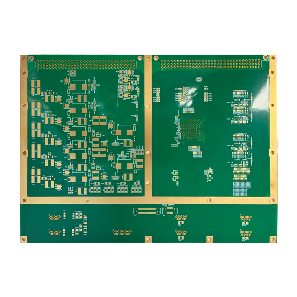
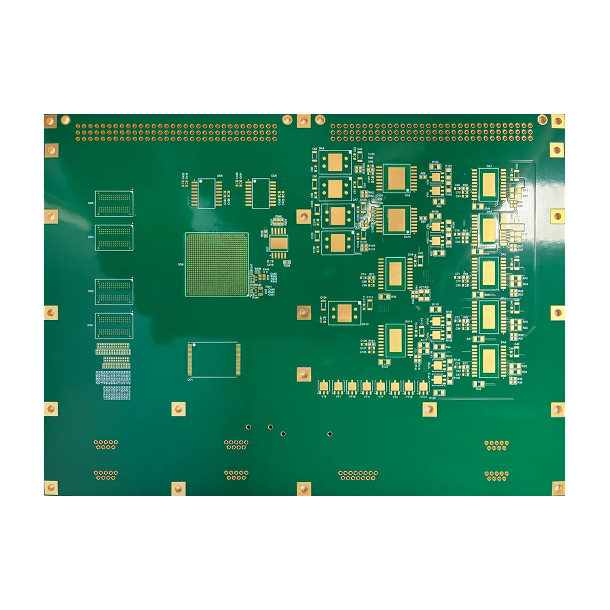
Bei diesem Produkt handelt es sich um ein 18-Schichtstarre Leiterplatte mit hoher Schichtanzahl mit einer genau kontrollierten Dicke von 1.86mm und Gesamtabmessungen von 165mm x 120 mm. Es nutzt branchenführende Megtron-7-Hochgeschwindigkeitslaminat mit geringem Verlust und verfügt über a 2-Mikrozoll (ca. 0.05µm) Elektrololes Nickel -Eintauchgold (ZUSTIMMEN) Oberflächenbeschaffung. Diese Spezifikation stellt eine erweiterte Stufe dar leistungsstark Leiterplattenherstellung, Entwickelt für Anwendungen, bei denen Signalintegrität erforderlich ist, Thermalmanagement, und Zuverlässigkeit stehen im Vordergrund.
2. Überlegungen zum kritischen Design
Entwerfen einer erfolgreichen 18-Lagen-Leiterplatte, insbesondere bei Hochgeschwindigkeitsmaterialien wie Megtron-7, erfordert eine sorgfältige Beachtung mehrerer Kernaspekte:
-
Stapeldesign: Ein rationaler Schichtaufbau ist entscheidend für die Impedanzkontrolle und die Reduzierung von Übersprechen. Ein typischer 18-Schicht-Stapel umfasst mehrere Signale, Leistung, und Masseebenen, um eine stabile Stromverteilung und klare Signalrückwege zu gewährleisten.
-
Impedanzkontrolle: Eine schnelle Signalübertragung erfordert Präzision Leiterplatte mit kontrollierter Impedanz Design. Die Breite und der Abstand der Leiterbahnen müssen anhand des Dk genau berechnet werden (Dielektrizitätskonstante) und Df (Dissipationsfaktor) von Megtron-7. Wir bieten professionelle Impedanzberechnungs- und Simulationsdienste.
-
Thermalmanagement: Die Plattendicke von 1,86 mm und der mehrschichtige Aufbau erfordern effektive Wärmepfade im Design, Beispielsweise werden thermische Vias verwendet, um interne Kupferschichten zu verbinden und so die Wärme von den Komponenten effizient abzuleiten.
-
Hochdichte Interconnect (HDI) Überlegungen: Hierbei handelt es sich zwar um ein Standard-Durchgangslochdesign, Sorgfältige Planung der Via-Typen (blind, begraben, Durchgangsloch) ist bei dieser Layer-Anzahl von entscheidender Bedeutung, um Stub-Effekte zu minimieren und Signalpfade zu optimieren.
3. Wie es funktioniert & Struktur
A Multi-Layer-PCB funktioniert wie ein hochintegriertes, dreidimensional “Straßennetz.” Elektrische Signale werden auf Kupferleitern übertragen (“Straßen”) auf der Oberfläche und den inneren Schichten, mit vertikalen Verbindungen zwischen den Schichten, die durch plattierte Durchgangslöcher hergestellt werden (“Austausch”). Dedizierte Strom- und Erdungsebenen sorgen für eine stabile Spannungsreferenz und Rauschabschirmung für das gesamte System. Das 18-Schicht starre PCB wird durch einen präzisen Laminierungsprozess geformt, Verbindung mehrerer Kernschichten und Prepreg-Blätter zu einer einzigen, Robustes Gerät mit hervorragenden elektrischen Eigenschaften. Es ist anspruchsvoll Leiterplattenstruktur ist die Grundlage für die Umsetzung komplexer Schaltungsfunktionalitäten.
4. Kernmaterialien & Schlüsselleistung
-
Materialien verwendet:
-
Laminieren: Megtron-7. Das ist eine Hochleistungsmaschine, verlustarmes kupferkaschiertes Laminat von Panasonic, bekannt für seine stabile Dielektrizitätskonstante (Dk ~3,3) und extrem niedrigem Verlustfaktor (Df ~0,001). Es ist für Anwendungen über 10 GHz und in Millimeterwellenfrequenzen optimiert.
-
Kupferfolie: Verwendet ein sehr niedriges Profil (VLP) oder umgekehrt behandelte Folie (RTF) zu minimieren “Hauteffekt” Verluste durch Signalübertragung auf rauen Kupferoberflächen.
-
Oberflächenbeschaffung: Elektrololes Nickel -Eintauchgold (ZUSTIMMEN, 2u”). Bietet eine ebene Oberfläche, ausgezeichnete Lötbarkeit, eine zuverlässige Kontaktschnittstelle (Geeignet für Goldfinger), und lange Haltbarkeit.
-
-
Hervorragende Leistung:
-
Überlegene Signalintegrität (UND): Der außergewöhnlich geringe Signalverlust stellt sicher, dass Hochgeschwindigkeitsimpulswellenformen unverzerrt bleiben.
-
Ausgezeichnete Leistungsintegrität (PI): Mehrere dedizierte Strom- und Erdungsebenen bieten eine sehr niedrige Impedanz des Stromverteilungsnetzwerks und eine hervorragende Entkopplung.
-
Hohe Zuverlässigkeit: Die Plattenstärke von 1,86 mm und die hochwertigen Materialien sorgen für eine hohe mechanische Festigkeit, Wärmewiderstand, und langfristige Umweltstabilität.
-
Stabile Impedanzkontrolle: Erreicht durch Materialkonsistenz und präzise Herstellungsprozesse.
-
5. Produktklassifizierung
Gemäß Industrie- und IPC-Standards, Dieses Produkt ist genau als klassifiziert:
-
Für Schichtzahl: Leiterplatte mit hoher Schichtanzahl (typischerweise definiert als 10+ Schichten).
-
Nach Materialtyp: Hochgeschwindigkeits-Hochfrequenz-Leiterplatte / Verlustarme Leiterplatte.
-
Durch Struktur: Starre PCB.
-
Nach Technologie: Leiterplatte mit kontrollierter Impedanz, ENIG Fertige Leiterplatte.
-
Nach Anwendungsklasse: Industriequalität / Hochleistungs-PCB in Telekommunikationsqualität.
6. Schlüsselmerkmale & Vorteile
-
Premium-Material: Aufgebaut Megtron-7-Hochgeschwindigkeitslaminat, Bereitstellung der physikalischen Grundlage für eine überlegene elektrische Leistung.
-
Hohe Komplexitätskapazität: Der 18-Schichtleiterplatte Das Design ermöglicht äußerst komplexe und dichte Schaltungslayouts.
-
Präzisionsfertigung: Strenge Toleranzkontrolle bei der Plattendicke von 1,86 mm und konsistent 2u” ZUSTIMMEN Oberflächenbehandlung.
-
Auf Geschwindigkeit ausgelegt: Durchgehend optimiert – vom Design über die Materialauswahl bis zur Verarbeitung – für Hochgeschwindigkeit digitale Schaltkreise Und HF-/Mikrowellenschaltungen.
7. Überblick über den Produktionsprozess
Der Herstellungsprozess für Leiterplatten mit hoher Schichtanzahl ist hochpräzise: Materialschneiden → Bildgebung der inneren Schicht & Ätzen → Automatisierte optische Inspektion (AOI) → Laminierung (Pressen mehrerer Innenschichtkerne mit Prepreg) → Bohren → Lochmetallisierung (Desmear, Stromlos & Elektrolytische Verkupferung) → Bildgebung der äußeren Schicht → Musterbeschichtung → Ätzen → Auftragen einer Lötmaske → Oberflächenbeschaffenheit (ZUSTIMMEN) → Profilführung → Elektrische Prüfung → Endkontrolle. Jeder Schritt erfordert eine strenge Kontrolle, insbesondere Schicht-zu-Schicht-Registrierung und Impedanzkontrolle.
8. Primäranwendungen & Anwendungsfälle
Das Hochleistungs-Leiterplatte ist die ideale Wahl für die folgenden erweiterten Anwendungen:
-
Hochgeschwindigkeitskommunikationsausrüstung: Core-Motherboards für optische 400G/800G-Module, High-End-Router, und Schalter.
-
Fortgeschrittenes Computing & Lagerung: Server-Motherboards, KI-Beschleunigerkarten, Hochgeschwindigkeits-Speicherarray (SSD) Controller-Boards.
-
Präzisionstest & Messgeräte: Interne Kernplatinen für High-End-Oszilloskope, Spektrumanalysatoren, und Signalgeneratoren.
-
Luft- und Raumfahrt & Verteidigungselektronik: Verarbeitungseinheiten in Radarsystemen und Satellitenkommunikationsnutzlasten.
-
Fortschrittliche medizinische Bildgebungsgeräte: Hochgeschwindigkeits-Datenerfassungs- und -verarbeitungskarten für Geräte wie MRT- und CT-Scanner.

Warum sollten Sie sich für UGPCB für Ihre 18-lagigen Megtron-7-Leiterplatten entscheiden??
Wir liefern mehr als nur ein Leiterplatte; Wir bieten eine umfassende Komplettlösung DFM (Design für die Herstellung) Rezension, Präzisionsherstellung, Und Zuverlässigkeitstest. Wir verfügen über umfassendes Fachwissen in jedem Detail hohe Schichtzahl Leiterplattenfertigung, Wir stellen sicher, dass Ihr Entwurf mit höchster Qualität und Zuverlässigkeit in die Realität umgesetzt wird.
Kontaktieren Sie uns noch heute für eine kostenlose technische Bewertung und ein wettbewerbsfähiges Angebot für Ihr Projekt. Machen Sie UGPCB zur robusten Grundlage für den Erfolg Ihres High-End-Produkts.


