

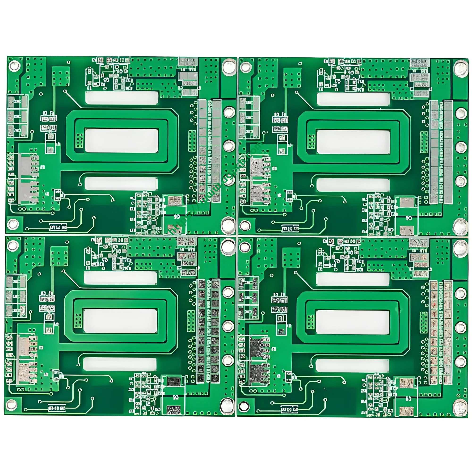
Produktübersicht: Was ist eine doppelseitige Nickel-Palladium-Gold-Leiterplatte??
Eine doppelseitige Nickel-Palladium-Gold-Leiterplatte (Auch als doppelseitige ENEPIG-Leiterplatte bekannt) ist ein Leiterplatte mit stromlosem Nickel, stromlosem Palladium-Immersionsgold (Enepic) Oberflächenveredelung auf beiden Seiten der Platte. Diese fortschrittliche Oberflächenbehandlung baut auf der traditionellen doppelseitigen PCB-Struktur auf, indem zwischen den Nickel- und Goldablagerungen eine Palladiumschicht hinzugefügt wird, Dadurch entsteht eine robuste dreischichtige Verbundoberfläche, die eine hervorragende Lötbarkeit bietet, Leistung beim Drahtbonden, und Umweltstabilität.
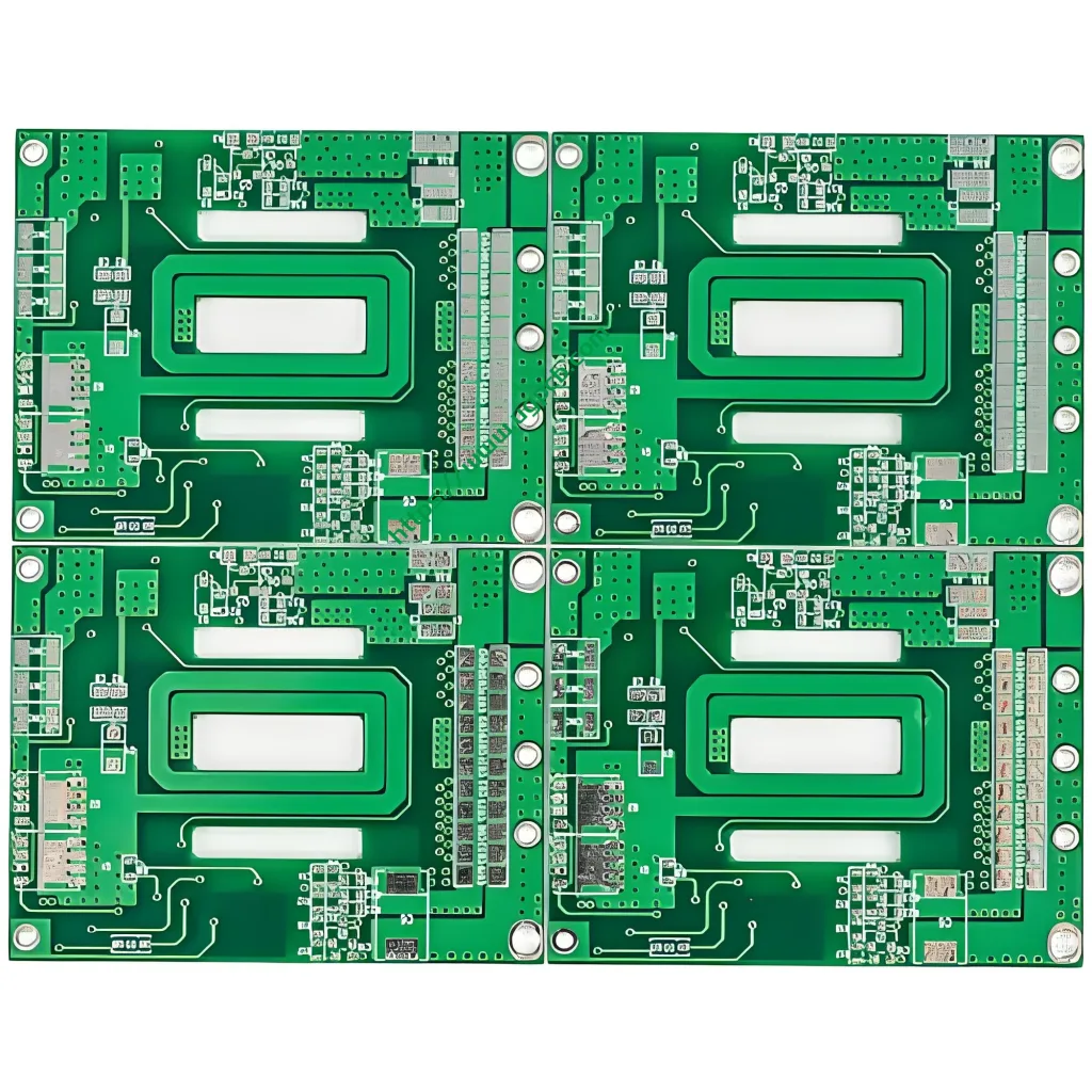
Die doppelseitige Nickel-Palladium-Gold-Leiterplatte von UGPCB verwendet kupferkaschiertes Kingboard KB6160A FR-4-Laminat als Basismaterial. Das Brett misst 49.6 × 32.8 mm mit einer Dicke von 1.6 mm und einer Kupferfoliendicke von 1 oz (etwa 35 μm). Die Lötmaske ist grün mit weißen Siebdruckzeichen. Mit einer minimalen Blende von 0.27 mm und eine Mindestlinienbreite/-abstand von 0.27 × 0.3 mm, Diese ENEPIG-Leiterplatte bietet Präzisionsfertigung kombiniert mit hochwertiger Oberflächenveredelung.
Die Nickel-Palladium-Gold-Leiterplatte gilt weithin als „universelle Oberflächenveredelung“ in der Elektronikindustrie. Es bedient ein breites Anwendungsspektrum, einschließlich Telekommunikation, Unterhaltungselektronik, Industrielle Steuerung, Sicherheitssysteme, Automobilelektronik, Netzteile, Smart-Home-Geräte, medizinische Ausrüstung, und Militär-/Luft- und Raumfahrtsysteme.
Wichtige technische Spezifikationen
| Parameter | Spezifikation |
|---|---|
| Laminieren | Kingboard KB6160A FR-4 |
| Brettdicke | 1.6 mm |
| Anzahl der Schichten | Doppelseitig |
| Brettgröße | 49.6 × 32.8 mm |
| Minimale Blende | 0.27 mm |
| Mindestlinienbreite/-abstand | 0.27 × 0.3 mm |
| Dicke der Kupferfolie | 1 oz (≈35 μm) |
| Oberflächenbeschaffung | Nickel-Palladium-Gold (Enepic) |
| Lötmaske / Legende | Grüne Lötmaske / Weißer Siebdruck |
Laminatdetails: KB6160A FR-4 kupferkaschiertes Laminat
KB6160A ist ein kupferkaschiertes FR-4-Hochleistungslaminat, hergestellt von Kingboard Laminates Holdings Ltd. Dieses Material wurde speziell für standardmäßige doppelseitige Leiterplatten entwickelt (PWB) Herstellung. Es entspricht dem Spezifikationsblatt IPC-4101/21. Zu den wichtigsten Eigenschaften gehören:
- UV -Blockierung (UVB) Fähigkeit: Verhindert die Lichtdurchlässigkeit während der Bildgebung, Verbesserung der Musterübertragungsgenauigkeit und -ausbeute
- Hervorragende Dimensionsstabilität: Gewährleistet Präzision im gesamten Herstellungsprozess
- Überragende Hitzebeständigkeit und mechanische Eigenschaften: Erfüllt die Anforderungen an Anwendungen mit hoher Zuverlässigkeit
- Glasübergangstemperatur (Tg): 135°C (DSC-Methode)
- Temperaturtemperatur thermische Zersetzung (Td): 305°C (TGA-Methode)
- Z-Achse CTE (a1/a2): 58 ppm/° C. (< Tg) / 286 ppm/° C. (> Tg)
- Dielektrizitätskonstante (Dk): 4.58
- Dissipationsfaktor (Df): 0.022
- Volumenwiderstand: 1 × 10⁸ MΩ-cm
- Feuchtigkeitsabsorption: 0.21%
- Entflammbarkeitsbewertung: UL94 V-0
(Die oben genannten Daten stammen aus dem technischen Datenblatt Kingboard KB6160A, mit Testmethoden gemäß den Standards der IPC-TM-650-Serie.)
Das ENEPIG-Oberflächenfinish: Eine ausführliche Erklärung
Was ist ENEPIG??
ENEPIG steht für Electroless Nickel Electroless Palladium Immersion Gold. Es handelt sich um eine stromlose chemische Oberflächenbehandlung, bei der nacheinander drei Metallschichten – Nickel – abgeschieden werden, Palladium, und Gold – auf die Kupferschaltung von a Leiterplatte.
Die dreischichtige Struktur von ENEPIG besteht aus:
- Untere Schicht – Chemisches Nickel (In): Dicke von 3–5 μm. Diese Schicht fungiert als Diffusionsbarriere, Verhindert die Migration von Kupfer an die Oberfläche und bietet gleichzeitig mechanischen Halt und eine Grundlage für das Löten.
- Mittlere Schicht – Stromloses Palladium (Pd): Dicke von 0,05–0,1 μm. Diese kritische Barriereschicht verhindert die Wechselwirkung zwischen Nickel und Gold, Beseitigung galvanischer Korrosion.
- Obere Schicht – Immersionsgold (Au): Dicke von 0,03–0,05 μm. Diese dünne Schicht bietet eine hervorragende Lötbarkeit und einen hervorragenden Oxidationsschutz.
Gemäß IPC-4556A (das Neueste 2025 Revision), Die Anforderungen an die Dicke der ENEPIG-Ablagerungen sind wie folgt spezifiziert:
- Nickelschicht: 3 μm zu 6 μm (gemessen bei durchschnittlich ± 4σ)
- Palladiumschicht: 0.05 μm zu 0.30 μm (gemessen bei durchschnittlich ± 4σ)
- Goldschicht: Minimum 0.030 μm, maximal 0.07 μm (gemessen bei unterdurchschnittlich − 4σ)
(Die oben genannten Dickenangaben basieren auf IPC-4556A, Spezifikation für stromloses Nickel/stromloses Palladium/Immersionsgold (Enepic) Beschichtung für Leiterplatten.)
Der ENEPIG-Prozessablauf
Die doppelseitigen Nickel-Palladium-Gold-Leiterplatten von UGPCB folgen einem standardisierten stromlosen Beschichtungsprozess:
Entfetten → Mikroätzen → Vortauchen → Aktivierung → Chemische Vernickelung → Chemische Palladiumbeschichtung → Tauchvergoldung → Trocknen
Jeder Prozessschritt umfasst mehrere Spülschritte, um die Qualität und Haftung der Beschichtung sicherzustellen. Die beteiligten chemischen Reaktionen umfassen sowohl Oxidations-Reduktions-Reaktionen als auch Verdrängungsreaktionen.
Kernvorteile doppelseitiger Nickel-Palladium-Gold-Leiterplatten
1. Vollständige Beseitigung des „Black Pad“-Defekts
Die ENIG (Elektrololes Nickel -Eintauchgold) Der Prozess leidet seit langem unter dem „Black Pad“-Defekt – einem Zustand, bei dem ein Goldangriff auf die Nickelschicht zu spröden Lötstellen und vorzeitigem Ausfall führt. ENEPIG löst dieses Problem durch die Einführung einer Palladium-Barriereschicht zwischen Nickel und Gold, Verhindert direkten Kontakt und verhindert Korngrenzenkorrosion. Branchendaten zeigen, dass ENEPIG das Auftreten von Black-Pads nahezu reduziert 90% im Vergleich zu ENIG. Unter extremen Temperaturwechselbedingungen, ENEPIG demonstriert bis zu 30% höhere Zuverlässigkeit als ENIG.
2. Überlegene Drahtbondfähigkeit
ENEPIG-Oberflächenveredelungen bieten eine hervorragende Bondleistung sowohl für Gold- als auch für Aluminiumdrähte. Die Palladiumschicht erweitert das Prozessfenster für das Golddrahtbonden, Dies ermöglicht zuverlässige Drahtbonds auch bei dünneren Goldablagerungen. In vielen Anwendungen, ENEPIG unterstützt Drahtbondfestigkeiten von mehr als 100 % 10 Gramm für Gold- und Aluminiumdrahtbonds. Dadurch eignen sich doppelseitige Nickel-Palladium-Gold-Leiterplatten besonders für Halbleiterverpackungen und Hybridmontageanwendungen, die Drahtbonden erfordern.
3. Hervorragende Lötbarkeit und mehrfache Reflow-Toleranz
ENEPIG-Oberflächenveredelungen bieten eine hervorragende Lötbarkeit sowohl mit bleihaltigen als auch mit bleifreien Loten (einschließlich SAC305-Legierung). ENEPIG-veredelte Leiterplatten halten bis zu 10 Reflow-Zyklen ohne wesentliche Verschlechterung.
4. Verlängerte Haltbarkeit
Dank der schützenden Palladiumschicht, ENEPIG-Oberflächenveredelungen bieten eine hervorragende Oxidations- und Korrosionsbeständigkeit. Dies führt zu einer deutlich längeren Haltbarkeit im Vergleich zu anderen Oberflächenveredelungen. Gemäß IPC-Richtlinien, ENEPIG-Oberflächen können die IPC-Kategorie erreichen 3 Haltbarkeit mindestens zwölf Monate.
5. Größere Designflexibilität
Im Gegensatz zu elektrolytischen Nickel-Gold-Verfahren, ENEPIG ist ein stromloses Verfahren, das keine Sammelschienen oder plattierten Leitungen erfordert. Dadurch können mehr Platinen gleichzeitig im selben Galvanisierbad bearbeitet werden, Erhöhung des Gesamtdurchsatzes. Zusätzlich, ENEPIG erlegt keine Routing-Einschränkungen auf, Bietet mehr Flexibilität für Schaltungsdesigns mit hoher Dichte.
Wie doppelseitige Nickel-Palladium-Gold-Leiterplatten funktionieren
Die synergistische Wirkung von drei Beschichtungsschichten
Die außergewöhnliche Leistung doppelseitiger Nickel-Palladium-Gold-Leiterplatten beruht auf der präzisen Synergie der drei Beschichtungsschichten:
① Nickelschicht (Ni-P-Legierung) – Die Foundation-Barriere
Die Nickelschicht dient als Grundlage der ENEPIG-Struktur. Seine Hauptfunktion besteht darin, die Diffusion von Kupferatomen zur Oberfläche zu blockieren, Verhindert die Bildung spröder intermetallischer Cu-Sn-Verbindungen (IMC) beim Löten oder bei Einwirkung hoher Temperaturen. Die Nickeldicke wird typischerweise auf 3–6 μm eingestellt, wobei der Phosphorgehalt strikt bei 7–9 % gehalten wird, um Härte und Korrosionsbeständigkeit auszugleichen.
② Palladiumschicht (Pd) – Die kritische Barriere- und Aktivierungsschicht
Die Palladiumschicht ist das entscheidende Merkmal, das ENEPIG von ENIG unterscheidet. Es fungiert als „Trennwand“.,„Verhinderung von Migration und Korngrenzenkorrosion zwischen Nickel und Gold. Die Palladiumschicht muss dick genug sein, um die Nickeldiffusion zur Goldoberfläche zu blockieren und eine übermäßige Korrosion der stromlosen Nickelabscheidung zu verhindern.
③ Goldschicht (Au) – Schutz und Lötbarkeit
Die dünne äußere Goldschicht schützt das Nickel vor Oxidation und sorgt gleichzeitig für einen geringen Kontaktwiderstand und eine hervorragende Lötbarkeit. Denn die Palladiumschicht sorgt für Isolation, Die Goldschicht in ENEPIG kann dünner gemacht werden (0.03–0,05 μm) ohne Kompromisse bei der Zuverlässigkeit einzugehen, Dies trägt dazu bei, die Materialkosten in gewissem Maße zu senken.
Klassifizierung doppelseitiger Nickel-Palladium-Gold-Leiterplatten
Die doppelseitige Nickel-Palladium-Gold-Leiterplatte von UGPCB kann wissenschaftlich in mehreren Dimensionen klassifiziert werden:
Nach Anzahl der Schichten
- Doppelseitige Leiterplatte: Auf beiden Seiten des Substrats sind leitende Schaltkreise verteilt, mit elektrischen Verbindungen, die durch plattierte Durchgangslöcher hergestellt werden (PTHS).
Nach Basismaterial
- FR-4 Epoxid-Glasgewebelaminat: Verwendung von Kingboard KB6160A, konform mit IPC-4101/21.
Nach Oberflächenbeschaffenheit
- Enepic (Elektrololes Nickel Elektrololless Palladium Immersion Gold) : Dreischichtige Verbundbeschichtungsstruktur.
Nach Anwendungsdomäne
- Hochzuverlässige Allzweck-Leiterplatte: Geeignet für die Telekommunikation, Automobilelektronik, medizinische Geräte, Luft- und Raumfahrt, Industrielle Steuerung, und mehr.
Durch Fertigungspräzision
- Präzisionsplatine: Mindestblende von 0.27 mm, Mindestlinienbreite/-abstand von 0.27 × 0.3 mm.
Ablauf des Herstellungsprozesses
Die Produktion doppelseitiger Nickel-Palladium-Gold-Leiterplatten von UGPCB folgt einem umfassenden Fertigungsworkflow:
Bühne 1: Untergrundvorbereitung
- Materialschnitt: Das kupferkaschierte Laminat KB6160A wird auf die erforderlichen Abmessungen zugeschnitten.
- Bohren: Mechanisches Bohren mit einer Mindestöffnung von 0.27 mm.
- Stromlose Kupferabscheidung & Plattenbeschichtung: Durchkontaktierte Metallisierung.
Bühne 2: Schaltungsbildung
- Musterübertragung: Trockenfilmlaminierung → Belichtung → Entwicklung.
- Schaltkreis Ätzen: Entfernen von überschüssigem Kupfer zur Bildung des Schaltkreismusters.
- AOI (Automatisierte optische Inspektion) : Sicherstellung der Schaltungsgenauigkeit.
Bühne 3: Lötmaske und Legende
- Lötmaskendruck: Auftragen von grüner Tinte zum Schutz der Schaltkreise und zur Verhinderung von Lötbrücken.
- Legendendruck: Weiße Siebdruckzeichen.
Bühne 4: Oberflächenbeschaffung (Enepic)
- Entfetten: Entfernung von Oberflächenverunreinigungen.
- Mikroätzung: Leichtes Ätzen der Kupferoberfläche zur Verbesserung der Haftung.
- Vortauchen: Vorbehandlung vor der Aktivierung.
- Aktivierung: Abscheidung einer katalytischen Palladiumkeimschicht auf Kupfer.
- Chemische Vernickelung: Abscheidung einer Nickelschicht (3–5 μm).
- Chemische Palladiumbeschichtung: Abscheidung einer Palladiumschicht (0.05–0,1 μm).
- Immersionsvergoldung: Aufbringung einer Goldschicht (0.03–0,05 μm).
- Trocknen: Fertigstellung der Oberflächenveredelung.
Bühne 5: Endinspektion
- Elektrische Tests: Gewährleistung der elektrischen Kontinuität und Isolierung.
- Visuelle Inspektion: Überprüfung der Oberflächenqualität.
- Verpackung & Versand.
Typische Anwendungen
Die doppelseitigen Nickel-Palladium-Gold-Leiterplatten von UGPCB werden in zahlreichen Branchen häufig eingesetzt:
Telekommunikationsausrüstung
- Basisstationen, Router, Schalter
- Hochfrequenz-Kommunikationsmodule, HF-Geräte
Kfz -Elektronik
- Motorsteuergeräte (ABDECKUNG)
- Infotainmentsysteme im Fahrzeug
- Adas (Fortgeschrittene Fahrerhilfesysteme)
- BMS (Batteriemanagementsysteme) für Fahrzeuge mit neuer Energie

Medizinprodukte
- Medizinische implantierbare Geräte
- Diagnoseinstrumente, Geräte zur Patientenüberwachung
Luft- und Raumfahrt & Verteidigung
- Raumfahrzeug- und Satellitenelektronik
- Flugkontrollsysteme
Industrielle Steuerung & Sicherheit
- Plc (Speicherprogrammierbare Steuerungen)
- Industrielle Motorantriebe
- Sicherheits- und Überwachungsausrüstung
Unterhaltungselektronik & Smart Home
- Smartphone-Motherboards
- Smart-Home-Steuerungsmodule
- Tragbare Geräte
Militär & Leistungselektronik
- Militärische elektronische Systeme
- Leistungsmodule, Leistungswandler
Warum sollten Sie sich für UGPCB für doppelseitige Nickel-Palladium-Gold-Leiterplatten entscheiden??
✅ Einhaltung der IPC-Standards
Die doppelseitigen Nickel-Palladium-Gold-Leiterplatten von UGPCB werden in strikter Übereinstimmung mit IPC-4556A hergestellt. Das Laminat KB6160A entspricht IPC-4101/21, Gewährleistung einer vollständigen Standardisierung vom Grundmaterial bis zur Oberflächenbeschaffenheit.
✅ Präzisionsfertigungskapazitäten
Mit einer minimalen Blende von 0.27 mm und Mindestlinienbreite/-abstand von 0.27 × 0.3 mm, UGPCB erfüllt die Anforderungen hochdichter Verbindungen (HDI) und Fine-Pitch-Komponentenmontage.
✅ Hohe Zuverlässigkeit
Die ENEPIG-Oberflächenveredelung reduziert schwarze Pad-Defekte nahezu 90% und liefert bis zu 30% höhere Zuverlässigkeit als ENIG bei extremen Temperaturschwankungen. Die Produkte halten mehreren Reflow-Zyklen stand und erfüllen die J-STD-Norm-003 Kategorie 3 Haltbarkeitsanforderungen.
✅ Professioneller technischer Support
Das UGPCB-Team bietet technischen Support für den gesamten Prozess, Von der Gerber-Dateiüberprüfung und Stücklistenoptimierung bis hin zur PCBA-Montage.
Anfragen & Bestellung
Bereit, Ihr Design in eine hochwertige doppelseitige Nickel-Palladium-Gold-Leiterplatte umzuwandeln?
📧 E-Mail: sales@ugpcb.com
📞 Telefon: +86-135 4412 8719
🌐 Website: www.ugpcb.com
📋 Bestellvorgang:
- Senden Sie Gerber-Dateien, Stückliste, und Konstruktionsdokumentation.
- Das Ingenieurteam von UGPCB führt DFM durch (Design für die Herstellung) Rezension.
- Auftragsbestätigung und Lieferplan.
- Herstellung und Qualitätskontrolle.
- Versand- und Logistikverfolgung.
Ob Sie brauchen PCB -Prototyping oder Massenproduktion, UGPCB ist bestrebt, hochwertige doppelseitige Nickel-Palladium-Gold-Leiterplatten und professionelle technische Dienstleistungen zu liefern.
Datenquellendeklaration
Die in diesem Dokument genannten technischen Daten und Standardspezifikationen stammen von den folgenden maßgeblichen Organisationen:
- IPC-4556A: Spezifikation für stromloses Nickel/stromloses Palladium/Immersionsgold (Enepic) Beschichtung für Leiterplatten (2025 Revision)
- IPC-4101/21: Spezifikation für Basismaterialien für starre und mehrschichtige Leiterplatten – das für KB6160A geltende Datenblatt
- Kingboard KB6160A Technisches Datenblatt (Kingboard Laminates Holdings Ltd.)
- IPC-TM-650: Handbuch zu Testmethoden – die Standardtestmethoden für die Messung von Materialeigenschaften
- J-Std-003: Lötbarkeitstests für Leiterplatten – der Prüfstandard für die Lötbarkeit
- Ul94: Norm für Tests zur Entflammbarkeit von Kunststoffmaterialien für Teile in Geräten und Geräten – Norm zur Entflammbarkeitsbewertung
Alle oben genannten Daten stammen aus den aufgeführten offiziellen Normen und technischen Dokumenten, Gewährleistung von Genauigkeit und Autorität.













