

Im Zeitalter der datenintensiven und ultraschnellen Signalübertragung, eine Leiterplatte (Leiterplatte) ist weit mehr als ein einfacher Komponententräger; Es ist die kritische Architektur, die die Leistungsgrenzen des Systems definiert. Für anspruchsvolle Anwendungen wie Hochgeschwindigkeitsnetzwerke, Künstliche Intelligenz, und fortschrittliche Testinstrumentierung, Standard-FR-4-Materialien reichen nicht aus. UGPCB geht mit unserem fortschrittlichen Produkt auf diesen Bedarf ein 22-Schicht-Mehrschicht-Leiterplatte aufgebaut Panasonic Megtron-6 R-5775G laminieren, Entwickelt, um den Herausforderungen der Hochfrequenz gerecht zu werden, geringer Verlust, und komplexe Vernetzung.
1.Die 22-lagige Megtron-6-Hochgeschwindigkeitsplatine von UGPCB Produktübersicht & Definition
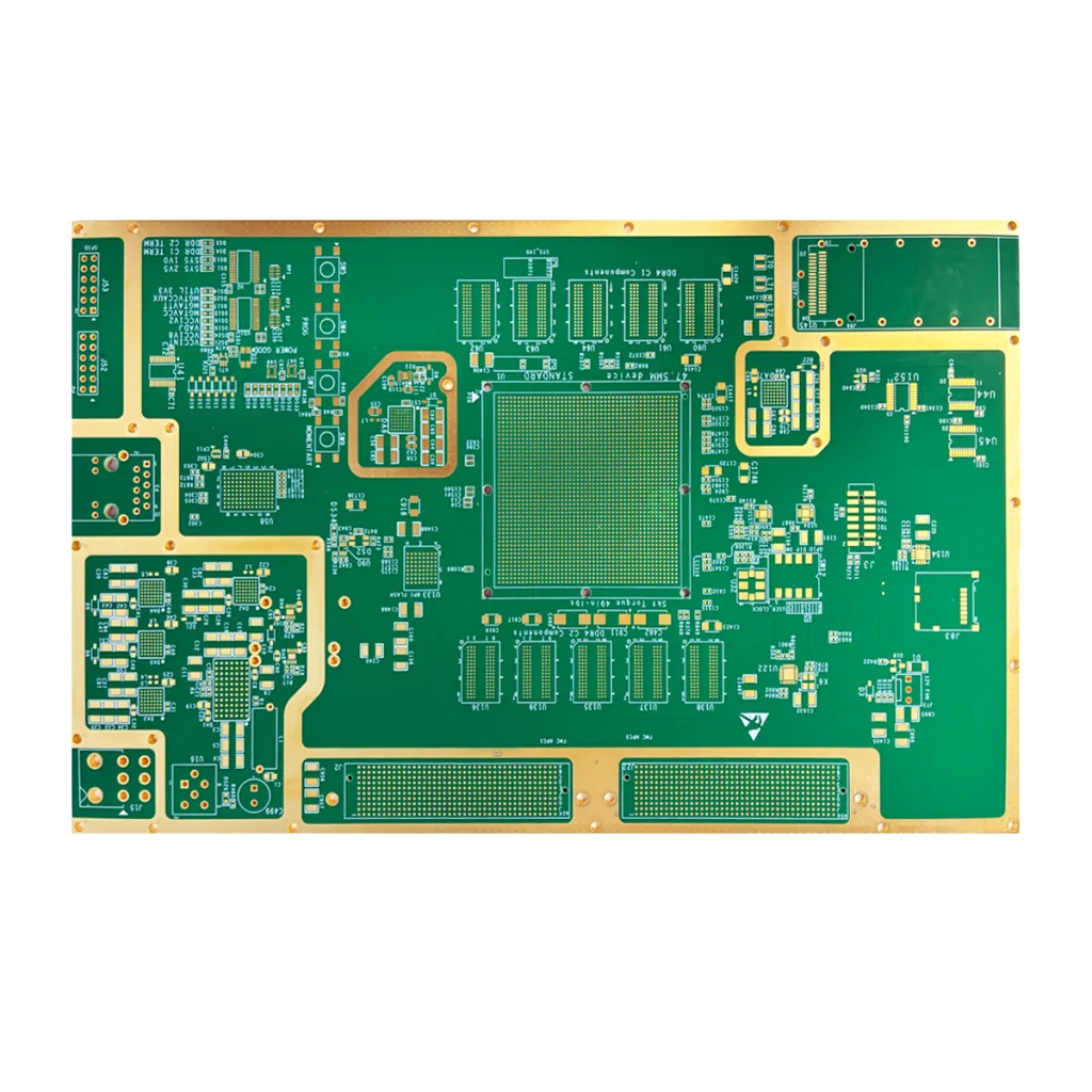
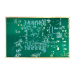
Bei diesem Produkt handelt es sich um ein 22-Schicht High-Density Interconnect (HDI) starre Leiterplatte. Sein Hauptvorteil liegt in der Verwendung einer Premium-Qualität, hohe Geschwindigkeit, verlustarmes Laminat – Panasonics Megtron-6 R-5775G. Kombiniert mit einer robusten Plattenstärke von 2,0 mm und Präzisionslaminiertechnologie, Es entsteht eine High-End-Verbindungsplattform, die Hochfrequenzsignale über 10 GHz mit außergewöhnlicher Signalintegrität und Leistungsintegrität verarbeiten kann.

2. Überlegungen zum kritischen Design
So ein Fortgeschrittenes entwerfen mehrschichtige Leiterplatte erfordert Konzentration auf:
-
Impedanzkontrolle: Präzise Berechnung und Steuerung der Single-Ended- und Differenzimpedanz, um eine konsistente Signalausbreitung innerhalb des Megtron-6-Dielektrikums sicherzustellen.
-
Stapeloptimierung: Die intelligente Anordnung der 22 leitfähige Schichten (22Schichten)– einschließlich Signal, Leistung, und Masseebenen – ist dabei entscheidend für die Maximierung der Abschirmung und die Minimierung des Übersprechens Leiterplatte mit hoher Schichtanzahl.
-
Thermalmanagement: Die Plattenstärke von 2,0 mm und der mehrschichtige Aufbau unterstützen die Wärmeverteilung. Jedoch, Der strategische Einsatz thermischer Vias bleibt für Hochleistungs-IC-Bereiche von entscheidender Bedeutung.
-
Hochfrequenz-Routing: Verwendung von Mikrostreifen- oder Streifenleitungskonfigurationen, Vermeiden Sie spitze Winkelkurven, und Nutzung der flachen Kupferfolie von Megtron-6, um Verluste durch den Skin-Effekt zu reduzieren.
3. Wie es funktioniert & Struktur
A Die Hauptfunktion der Leiterplatte besteht darin, elektrische Konnektivität und Signalübertragung zwischen Komponenten über geätzte Kupferleiterbahnen auf einem isolierenden Substrat bereitzustellen. Das 22-Layer -PCB -Platine Die Struktur ähnelt einer präzisen “mehrschichtiges Sandwich”:
-
Innere Schichten: Verwenden Sie M/HOZ (etwa 1/1 oz oder 35µm) Kupfer für Kernstrom, Bodenebenen, und etwas internes Signalrouting.
-
Außenschichten: Verwenden 1/1 Unzen Kupfer für die Montage von Primärkomponenten und die Verlegung kritischer Signalleiterbahnen.
-
Dielektrische Schichten: Alle isolierenden Prepreg-Materialien sind Panasonic Megtron-6 R-5775G, dessen niedrige Dielektrizitätskonstante (Dk) und Dissipationsfaktor (Df) sorgen für eine überragende Hochgeschwindigkeits-Signalübertragung.
-
Oberflächenbeschaffung: Elektrololes Nickel -Eintauchgold (ZUSTIMMEN) bei 2 Mikrozoll (2u”). Dadurch entsteht eine Wohnung, lötbare Oberfläche, ausgezeichnete Oxidationsbeständigkeit, und gute Drahtbondfähigkeit, Ideal für hochdichte BGA-Gehäuse und HF-Anschlüsse.
4. Kernmaterial: Panasonic Megtron-6 R-5775G
Das ist das Herzstück davon fortschrittliches PCB-Material. Megtron-6 ist die nächste Generation von Panasonic, hohe Geschwindigkeit, Serie aus verlustarmen Leiterplattenmaterialien.
-
Schlüsselleistung: Verfügt über eine extrem niedrige Dielektrizitätskonstante (Dk~3,5) und extrem niedriger Verlustfaktor (Df~0,0015 bei 10 GHz), übertrifft den Standard FR-4 deutlich. Seine hohe Glasübergangstemperatur (Tg) gewährleistet eine hervorragende thermische Stabilität und Maßhaltigkeit bei Hochtemperatur-Reflow-Lötprozessen.
-
Anwendungstauglich: Optimiert für digitale Hochgeschwindigkeitssignale (10Gbit/s+ bis 56/112 Gbit/s) und Millimeterwellen-HF-Anwendungen.
| Artikel | Testmethode | Zustand | Einheit | Megtron6 R-5775(N) Low DK Glass Tuch |
Megtron6 R-5775 Normales Glas Tuch |
|
| Glasübergangstemperatur.(Tg) | DSC | A | °C | 185 | 185 | |
| Wärmezersetzungstemp.(Td) | TGA | A | °C | 410 | 410 | |
| CTE x-Achse | A1 | IPC-TM-650 2.4.24 | A | ppm/° C. | 14-16 | 14-16 |
| Cte y-Achse | 14-16 | 14-16 | ||||
| CTE Z-Achse | A1 | IPC-TM-650 2.4.24 | A | 45 | 45 | |
| A2 | 260 | 260 | ||||
| T288(mit Kupfer) | IPC-TM-650 2.4.24.1 | A | min | >120 | >120 | |
| Dielektrizitätskonstante(Dk) | 12GHz | Ausgeglichener Typ Rundscheibe Resonator |
C-24/23/50 | - | 3.4 | 3.6 |
| Dissipationsfaktor(Df) | 0.004 | 0.004 | ||||
| Wasseraufnahme | IPC-TM-650 2.6.2.1 | D-24/23 | % | 0.14 | 0.14 | |
| Biegermodul | Füllen | Jis c 6481 | A | GPA | 18 | 19 |
| Schälfestigkeit* | 1oz(35μm) | IPC-TM-650 2.4.8 | A | kN/m | 0.8 | 0.8 |
5. Schlüsselmerkmale & Leistung
-
Extrem geringer Signalverlust: Megtron-6-Material sorgt für maximale Effizienz bei der Hochfrequenzsignalübertragung bei minimaler Dämpfung.
-
Ausgezeichnete Thermik & Dimensionsstabilität: Ein hoher Tg-Wert in Kombination mit einer 2,0 mm dicken Platte eignet sich für hohe Temperaturen, Hochleistungsanwendungsumgebungen.
-
High-Density-Verbindungsfähigkeit: Das 22-Lagen-Design bietet reichlich Routing-Kanäle, Unterstützung komplexer Verbindungen für große Chips (z.B., FPGAs, GPUs).
-
Präzise Impedanz & Layer-zu-Layer-Registrierung: Ausgereifte Herstellungsprozesse garantieren eine gleichbleibende elektrische Leistung über den gesamten Zeitraum mehrschichtige Leiterplatte.
-
Hervorragende Lötbarkeit & Bindung: Die 2u” Die ENIG-Oberfläche gewährleistet äußerst zuverlässige Lötverbindungen und eignet sich für die präzise SMT-Bestückung.
6. Wissenschaftliche Klassifikation & Primäranwendungen
-
Wissenschaftliche Klassifikation:
-
Für Schichtzahl: High-Multilayer-Leiterplatte (Typischerweise >10 Schichten).
-
Durch Material: Hochgeschwindigkeits-PCB / Hochfrequenz-PCB / Verlustarme Leiterplatte.
-
Nach Technologie: HDI PCB (Vorbehaltlich spezifischer Designmerkmale wie Blind-/Buried Vias).
-
Durch Starrheit: Starre PCB.
-
-
Primäranwendungen & Anwendungsfälle:
-
Hochgeschwindigkeits-Netzwerkausrüstung: Kern-Backplanes und Motherboards für optische 400G/800G-Module, High-End-Router, und Schalter.
-
Fortgeschrittenes Computing & Lagerung: AI-Serverboards, Hochleistungs-Computing (HPC) Cluster, SSD-Controller-Boards für Unternehmen.
-
Luft- und Raumfahrt & Radarsysteme: HF-Frontends und Signalverarbeitungseinheiten für Avionikkommunikation und Phased-Array-Radarsysteme.
-
Erweiterter Test & Messgeräte: Mainboards in Hochgeschwindigkeitsoszilloskopen, Spektrumanalysatoren, und Signalgeneratoren.
-
7. Übersicht über den Produktionsfluss
UGPCB hält sich an eine strenge Einhaltung PCB-Herstellungsprozess Qualität zu gewährleisten:
Materialschneiden → Bildgebung der inneren Schicht → Laminierung (22-Schichtausrichtung & Bindung) → Bohren → Lochmetallisierung → Bildgebung der äußeren Schicht → Musterbeschichtung → Ätzen → Auftragen einer Lötmaske → ENIG-Oberflächenbearbeitung → Fräsen / Bewertung → Elektrische Prüfung → Endkontrolle (AOL)
Jeder Schritt wird durch hochpräzise Geräte unterstützt, mit mehreren integrierten Qualitätskontrollpunkten PCB-Herstellungsprozess, dies sicherzustellen 22-Schicht Megtron-6 PCB erfüllt höchste Ansprüche vom Design bis zur Lieferung.
Lassen Sie nicht zu, dass Basismaterialien Ihre innovativen Designs einschränken.
Ganz gleich, ob Sie Kommunikationshardware der nächsten Generation entwickeln oder sich den Herausforderungen des Frontier Computing stellen, UGPCB 22-Layer-Hochleistungs-PCB-Lösung ist Ihre zuverlässige Hardware-Basis. Wir bieten nicht nur ein Produkt, aber umfassende Unterstützung von Beratung zum PCB-Design bis hin zum Rapid Prototyping und der Serienfertigung.
Klicken Sie hier, um ein Angebot anzufordern und eine fachkundige technische Dokumentation zu erhalten. Unterstützen Sie Ihr Projekt mit einem überlegenen Kern!


