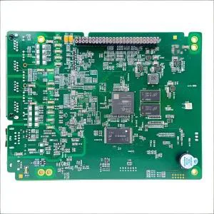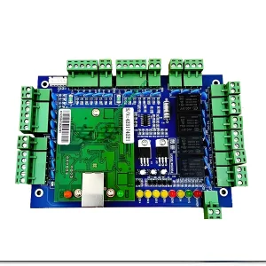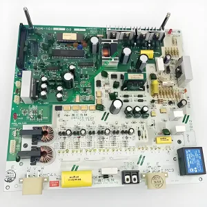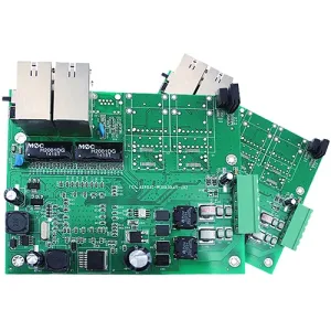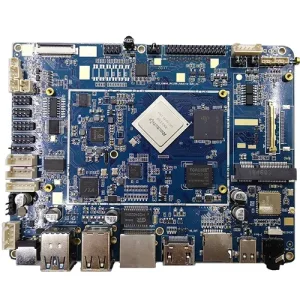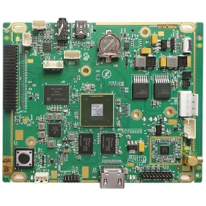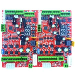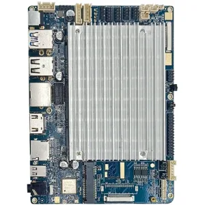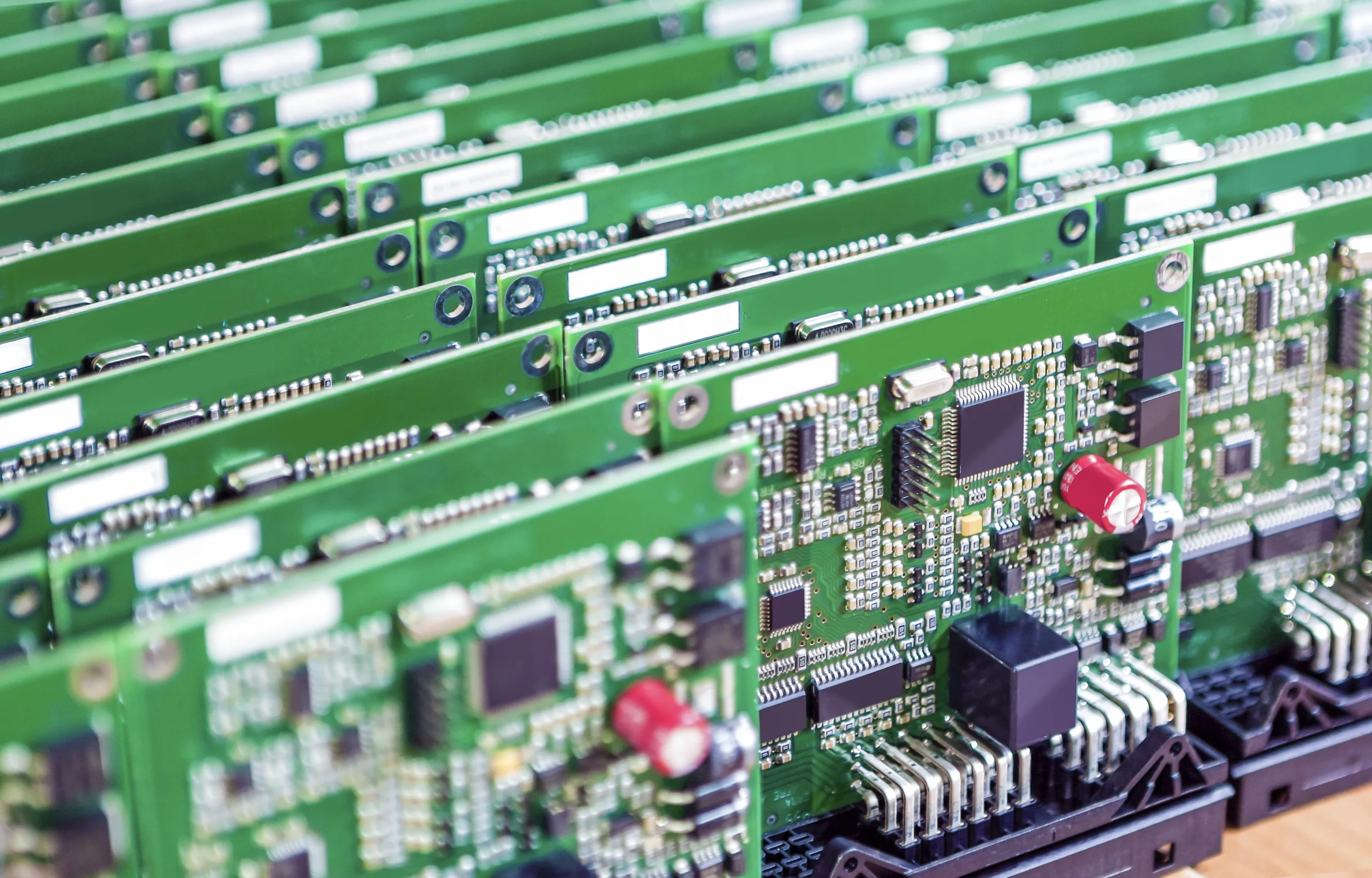
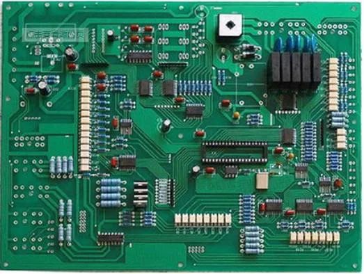
Conjunto de PCB para equipos de comunicación, el nombre chino es placa de circuito impreso, También conocido como placa de circuito impreso., Es un componente electrónico importante., un soporte para componentes electrónicos, y un soporte para conexiones eléctricas de componentes electrónicos.. Porque está fabricado mediante impresión electrónica., se llama un “impreso” tarjeta de circuitos.
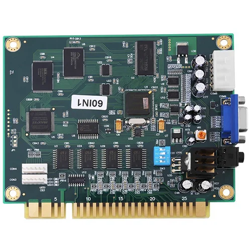
Efecto
Después de que los equipos electrónicos adopten tableros impresos, debido a la consistencia de tableros impresos similares, Se evitan errores en el cableado manual., e inserción o colocación automática de componentes electrónicos, soldadura automática, Y se puede realizar una detección automática para garantizar la calidad de los equipos electrónicos.. , Mejorar la productividad laboral, reducir costos, y facilitar el mantenimiento.
Desarrollar
El ensamblaje de placas de circuito impreso se ha desarrollado desde una sola capa hasta dos caras., multicapa y flexible, y aún mantienen sus propias tendencias de desarrollo.. Debido al continuo desarrollo hacia la alta precisión, alta densidad y alta confiabilidad, reducción continua de tamaño, reducción de costes y mejora del rendimiento, Los tableros impresos aún mantienen una gran vitalidad en el desarrollo de futuros equipos electrónicos..
Un resumen de las discusiones nacionales y extranjeras sobre la tendencia de desarrollo futuro de la tecnología de fabricación de tableros impresos es básicamente el mismo., eso es, a alta densidad, alta precisión, apertura fina, alambre fino, tono fino, alta confiabilidad, multicapa, transmisión de alta velocidad, peso ligero, Desarrollando hacia la delgadez, También se está desarrollando en la dirección de mejorar la productividad., reduciendo costos, reduciendo la contaminación, y adaptarse a la producción multivariedad y en lotes pequeños. El nivel de desarrollo técnico de los circuitos impresos generalmente está representado por el ancho de línea., abertura, y espesor de la placa/relación de apertura de la placa de circuito impreso.
Fuente
El creador de la placa de circuito impreso fue el austriaco Paul Eisler., quien lo usó por primera vez en una radio en 1936. En 1943, Los estadounidenses aplicaron principalmente esta tecnología a las radios militares.. En 1948, Estados Unidos reconoció oficialmente esta invención para uso comercial.. Las placas de circuito impreso sólo se han utilizado ampliamente desde mediados de la década de 1950..
Antes de la aparición de PCB, la interconexión entre componentes electrónicos se realizó mediante conexión directa de cables. Hoy, Los cables existen sólo para aplicaciones experimentales en el laboratorio.; Las placas de circuito impreso han ocupado definitivamente una posición de control absoluto en la industria electrónica..
Proceso de producción de PCB
Póngase en contacto con el fabricante
Primero necesitas contactar al fabricante., y luego registrar el número de cliente, entonces alguien te cotizará, hacer un pedido, y seguir el progreso de la producción..
Corte
Objetivo: Según los requisitos de los datos de ingeniería MI., cortar las hojas grandes que cumplen con los requisitos en pedazos pequeños para producir hojas. Pequeñas piezas de chapa que cumplen con los requisitos del cliente..
Proceso: hoja grande → corte según los requisitos de MI → hoja rizada → filete de cerveza/molienda de bordes → salida de la hoja
Perforación
Objetivo: Según los datos de ingeniería., taladre el diámetro del orificio deseado en la posición correspondiente del material de la lámina que cumpla con el tamaño requerido.
Proceso: Stacking pins→upper board→drilling→lower board→inspect\repair
Cobre de inmersión
Objetivo: El cobre por inmersión consiste en depositar una fina capa de cobre en la pared del orificio aislante mediante un método químico..
Proceso: Molienda gruesa → placa colgante → línea automática de cobre sumergido → placa inferior → inmersión en % diluir H2SO4 → cobre espesado
Transferencia gráfica
Objetivo: La transferencia gráfica consiste en transferir la imagen de la película de producción al tablero.
Proceso: (proceso de aceite azul): Tablero de molienda → impresión de la primera cara → secado → impresión de la segunda cara → secado → exposición → fotografía → control; (proceso de película seca): Tablero de cáñamo → película de prensado → parada → par de bits → exposición → reposo → desarrollo → control
Chapado gráfico
Objetivo: La galvanoplastia de patrón consiste en galvanizar una capa de cobre con un espesor requerido y una capa de oro-níquel o estaño con un espesor requerido en la piel de cobre expuesta del patrón del circuito o en la pared del orificio..
Proceso: placa superior → desengrasado → lavado con agua dos veces → micrograbado → lavado con agua → decapado → revestimiento de cobre → lavado con agua → decapado → estañado → lavado con agua → placa inferior
Retirando la película
Objetivo: Utilice una solución de NaOH para eliminar la capa de revestimiento antichapado y exponer la capa de cobre sin línea..
Proceso: película de agua: insertar el marco → remojar en álcali → enjuagar → fregar → pasar la máquina; película seca: poner tablero → pasar máquina
Aguafuerte
Objetivo: El grabado consiste en utilizar un método de reacción química para corroer la capa de cobre de las piezas que no son del circuito..
aceite verde
Objetivo: El aceite verde sirve para transferir el patrón de la película de aceite verde a la placa para proteger el circuito y evitar que el estaño entre en el circuito al soldar piezas.
Proceso: Tablero de molienda → impresión de aceite verde fotosensible → tabla de curling → exposición → desarrollo de sombra; tablero de molienda → imprimir el primer lado → tablero para hornear → imprimir el segundo lado → tablero para hornear
Personajes
Objetivo: Los caracteres se proporcionan como una marca fácil de reconocer.
Proceso: Después de terminar el aceite verde → enfriar y reposar → ajustar la pantalla → imprimir caracteres → terminar el curio
Dedos dorados
Objetivo: Plating a layer of nickel\gold with the required thickness on the plug finger to make it more hard and wear-resistant
Proceso: tablero → desengrasado → lavado con agua dos veces → micrograbado → lavado con agua dos veces → decapado → cobreado → lavado con agua → niquelado → lavado con agua → chapado en oro
hojalata (un proceso paralelo)
Objetivo: HASL consiste en rociar una capa de plomo y estaño sobre la superficie de cobre expuesta que no está cubierta con aceite resistente a la soldadura para proteger la superficie de cobre de la corrosión y la oxidación., para garantizar un buen rendimiento de soldadura.
Proceso: micrograbado → secado al aire → precalentamiento → recubrimiento de colofonia → recubrimiento de soldadura → nivelación con aire caliente → enfriamiento por aire → lavado y secado al aire
formando
Objetivo: Mediante estampado de moldes o máquinas herramienta CNC para formar la forma requerida por los clientes.. Gongos organicos, tableros de cerveza, gongs de mano, y cortado a mano
Explicación: La precisión del tablero de la máquina de gong de datos y del tablero de cerveza es mayor., seguido por el gong de mano, y el tablero cortado a mano solo puede hacer algunas formas simples.
Prueba
Objetivo: A través de 100% pruebas electrónicas, Detectar defectos que afectan la funcionalidad, como circuitos abiertos y cortocircuitos que son difíciles de detectar visualmente..
Proceso: molde superior → colocación de tableros → prueba → calificado → inspección visual FQC → no calificado → reparación → prueba de devolución → OK → REJ → chatarra
Inspección final
Objetivo: A través de 100% inspección visual de defectos de apariencia del tablero, y reparar defectos menores, para evitar la salida de placas problemáticas y defectuosas.
Flujo de trabajo específico: Material entrante → datos de verificación → inspección visual → calificado → control puntual de FQA → calificado → embalaje → no calificado → procesamiento → verificar OK
Tendencias de la industria
La industria de PCB se está desarrollando rápidamente
Desde la reforma y apertura, China ha atraído una transferencia a gran escala de industrias manufactureras europeas y americanas debido a sus políticas preferenciales en términos de recursos laborales., mercados, e inversión. desarrollo de industrias relacionadas. Según las estadísticas de la CPCA de China, en 2006 Se alcanzó la producción real de PCB de mi país. 130 millones de metros cuadrados, con un valor de salida de 12.1 mil millones de dólares estadounidenses, contabilidad de 24.90% del valor de salida global de PCB, Superando a Japón para convertirse en el número uno del mundo.. De 2000 a 2006, se alcanzó la tasa de crecimiento anual promedio del mercado de PCB de China 20%, muy por encima del promedio mundial. La crisis financiera mundial en 2008 tuvo un gran impacto en la industria de PCB, pero no causó un golpe catastrófico a la industria de PCB de China.. Estimulado por la política económica nacional, La industria de PCB de China experimentó una recuperación total en 2010. En 2010, Se alcanza el valor de producción de PCB de China 19.971 mil millones de dólares estadounidenses . Prismark predice que China mantendrá una tasa de crecimiento anual compuesta de 8.10% entre 2010 y 2015, que es mayor que la tasa de crecimiento promedio global de 5.40%.
La distribución regional es desigual
La industria de PCB de China se distribuye principalmente en el sur y el este de China.. La suma de los dos llega 90% del pais, y el efecto de aglomeración industrial es evidente. Este fenómeno está relacionado principalmente con el hecho de que las principales bases de producción de la industria electrónica de China se concentran en el delta del río Perla y el delta del río Yangtze..
Distribución de aplicaciones posteriores de PCB
La distribución de aplicaciones posteriores en la industria de PCB de China se muestra en la siguiente figura.. La electrónica de consumo representó la mayor proporción, alcanzando 39%, seguido por las computadoras, contabilidad de 22%, contabilidad de comunicaciones para 14%, control industrial/instrumentos médicos que contabilizan 14%, contabilidad de la electrónica del automóvil 6%, y contabilidad de defensa nacional y aeroespacial 5%.
Tecnología atrasada
Aunque China es ahora el número uno del mundo en términos de escala industrial, todavía está por detrás del nivel avanzado del mundo en términos del nivel técnico general de la industria de PCB. En términos de estructura del producto., Los tableros multicapa representan la mayor parte del valor de salida., pero la mayoría de ellos son productos de gama baja con menos de 8 capas. IDH, tableros flexibles, etc.. tener una cierta escala, pero no son comparables a productos extranjeros avanzados como Japón en términos de contenido técnico.. Hay una brecha, Y hay muy pocas empresas en China que puedan producir sustratos de circuitos integrados con el mayor contenido técnico..
Clasificación
Clasificación según el número de capas del circuito.: dividido en tableros de una sola cara, tableros de doble cara y tableros multicapa. Los tableros multicapa comunes son generalmente tableros de 4 capas o tableros de 6 capas., y los tableros multicapa complejos pueden alcanzar docenas de capas.
Hay tres tipos principales de divisiones de placas PCB.:
un solo lado
La placa de una cara está en la PCB más básica., las piezas están concentradas en un lado, y los cables se concentran en el otro lado (cuando hay componentes de parche, es del mismo lado que los cables, y el dispositivo enchufable está en el otro lado). Porque los cables solo aparecen en un lado., Esta PCB se llama placa de una sola cara. (De una sola cara). Porque la placa única tiene muchas restricciones estrictas en el circuito de diseño. (porque solo hay un lado, el cableado no puede cruzar sino que debe recorrer un camino separado), entonces solo los primeros circuitos usan este tipo de placa.
Panel doble
Las placas de circuito de doble cara tienen cableado en ambos lados., pero usar los cables en ambos lados, Debe haber conexiones de circuito adecuadas entre los dos lados.. Este “puente” entre circuitos se llama vía. El orificio guía es un pequeño orificio lleno o recubierto de metal en la PCB., que se puede conectar a los cables en ambos lados. Porque el área del panel de doble cara es dos veces mayor que la del panel de una sola cara., el panel de doble cara resuelve la dificultad de intercalar el cableado en el panel de una cara (se puede conducir al otro lado a través de agujeros), y es más adecuado para su uso en circuitos que son más complicados que el panel de una sola cara.
Tablero multicapa
Para aumentar el área que se puede cablear, Los tableros multicapa utilizan más tableros de cableado de una o dos caras.. Utilice uno de doble cara como capa interior., dos de una cara como capa exterior o dos de doble cara como capa interior, dos de una cara como capa exterior de la placa de circuito impreso, A través del sistema de posicionamiento y el material de unión aislante se alternan entre sí y el patrón conductor. Las placas de circuito impreso interconectadas de acuerdo con los requisitos de diseño se convierten en placas de circuito impreso de cuatro y seis capas., También conocidas como placas de circuito impreso multicapa.. El número de capas de la placa no significa que existan varias capas de cableado independientes.. En casos especiales, Se agregarán capas vacías para controlar el grosor del tablero.. Generalmente, el número de capas es par e incluye las dos capas más externas. La mayoría de las placas base tienen una estructura de 4 a 8 capas, pero es técnicamente posible lograr una placa PCB con casi 100 capas. La mayoría de las grandes supercomputadoras utilizan placas base bastante multicapa., sino porque tales computadoras ya pueden ser reemplazadas por grupos de muchas computadoras comunes, Los tableros súper multicapa han ido quedando poco a poco en desuso.. Porque las capas de la PCB están estrechamente integradas, generalmente no es fácil ver el número real, pero si miras de cerca la placa base, todavía puedes verlo.
Características
La razón por la que la PCB se puede utilizar cada vez más es porque tiene muchas ventajas únicas., que se resumen a continuación.
Posible alta densidad. Durante décadas, La alta densidad de las placas impresas se ha podido desarrollar con la mejora de la integración de circuitos integrados y el avance de la tecnología de montaje..
alta confiabilidad. A través de una serie de inspecciones, pruebas y pruebas de envejecimiento, Se puede garantizar que la PCB funcionará de manera confiable durante mucho tiempo. (periodo de uso, generalmente 20 años).
Diseñabilidad. Para diversos requisitos de rendimiento de PCB (eléctrico, físico, químico, mecánico, etc.), El diseño de tableros impresos se puede realizar mediante la estandarización del diseño., normalización, etc., con poco tiempo y alta eficiencia.
producibilidad. Con una gestión moderna, normalización, escala (cantidad), La automatización y otras producciones se pueden llevar a cabo para garantizar la consistencia de la calidad del producto..
Capacidad de prueba. Un método de prueba relativamente completo, estándar de prueba, Se han establecido varios equipos e instrumentos de prueba para detectar e identificar la calificación y la vida útil de los productos de PCB..
ensamblabilidad. Los productos de PCB no solo son convenientes para el ensamblaje estandarizado de varios componentes, Pero también puede ser una producción en masa automatizada y a gran escala.. Al mismo tiempo, PCB y varios componentes de ensamblaje de componentes también se pueden ensamblar para formar componentes más grandes., sistemas, e incluso máquinas completas.
Mantenibilidad. Dado que los productos de PCB y diversas piezas de ensamblaje de componentes se diseñan y producen de manera estandarizada, Estas piezas también están estandarizadas.. Por lo tanto, una vez que el sistema falla, se puede reemplazar rápidamente, cómoda y flexiblemente, y el sistema se puede restaurar rápidamente para funcionar. Por supuesto, se pueden dar más ejemplos. Como hacer que el sistema sea miniaturizado y liviano., y transmisión de señal de alta velocidad.
Clasificación blanda y dura.
Dividido en placas de circuito rígido y placas de circuito flexible., tableros blandos y duros. Generalmente, La PCB que se muestra en la primera imagen a continuación se llama rígida. (Rígido) tarjeta de circuito impreso, y la línea de conexión amarilla en la segunda imagen se llama flexible (o flexible) tarjeta de circuito impreso. La diferencia intuitiva entre PCB rígido y PCB flexible es que el PCB flexible se puede doblar. Los espesores comunes de los PCB rígidos son 0,2 mm., 0.4milímetros, 0.6milímetros, 0.8milímetros, 1.0milímetros, 1.2milímetros, 1.6milímetros, 2.0milímetros, etc.. El espesor común de la PCB flexible es de 0,2 mm., y el lugar donde se van a soldar las piezas se agregará con una capa espesa detrás. El espesor de la capa engrosada varía de 0,2 mm a 0,4 mm.. El propósito de comprenderlos es proporcionar a los ingenieros estructurales una referencia espacial al diseñar.. Los materiales comunes para PCB rígidos incluyen: laminados de papel fenólico, laminados de papel epoxi, laminados de fieltro de vidrio de poliéster, laminados de tela de vidrio epoxi; Los materiales de PCB flexibles comúnmente incluyen: película de poliéster, película de poliimida amina, película de etileno propileno fluorado.
Materia prima
El laminado revestido de cobre es el material de sustrato para fabricar placas de circuito impreso.. Se utiliza para soportar varios componentes y realizar conexiones eléctricas o aislamiento eléctrico entre ellos..
Placa de aluminio
Sustrato de aluminio para PCB (El disipador de calor a base de metal incluye sustrato de aluminio., sustrato de cobre, y sustrato de hierro) es una placa de aleación de alta plasticidad de la serie Al-Mg-Si de baja aleación (ver la estructura a continuación), que tiene buenas propiedades de conductividad térmica y aislamiento eléctrico y rendimiento de mecanizado, ahora el sustrato de aluminio principal Fosslat.
Procesamiento de contactos
La pintura verde resistente a la soldadura cubre la mayor parte de la superficie de cobre del circuito., y sólo los contactos terminales para la soldadura de componentes, Las pruebas eléctricas y la inserción de la placa de circuito están expuestas.. Se debe agregar una capa protectora adecuada a este terminal para evitar óxidos en el terminal conectado al ánodo. (+) durante el uso a largo plazo, lo que afectará la estabilidad del circuito y causará problemas de seguridad..
[Chapado en oro duro] Una capa de níquel y una capa de oro altamente químicamente pasiva están revestidas en el terminal enchufable de la placa de circuito. (comúnmente conocido como dedo de oro) para proteger el terminal y proporcionar un buen rendimiento de conexión. Contiene una cantidad adecuada de cobalto., que tiene excelentes propiedades de resistencia al desgaste.
[tus problemas] El terminal de soldadura de la placa de circuito está cubierto con una capa de aleación de estaño y plomo mediante nivelación con aire caliente para proteger el terminal de la placa de circuito y proporcionar un buen rendimiento de soldadura..
[Pre-soldadura] El punto de soldadura de la placa de circuito se cubre con una capa de película de soldadura previa antioxidante en forma de teñido por inmersión., que protege temporalmente el punto de soldadura antes de soldar y proporciona una superficie de soldadura relativamente plana para un buen rendimiento de soldadura.
[Tinta de carbono] Se imprime una capa de tinta de carbón en los terminales de contacto de la placa de circuito mediante serigrafía para proteger los terminales y proporcionar un buen rendimiento de conexión..
corte de forma
Cortar la placa de circuito en las dimensiones requeridas por el cliente con una máquina formadora CNC. (o troqueladora). al cortar, use alfileres para fijar la placa de circuito en la cama (o molde) a través de los orificios de posicionamiento previamente perforados. Después de cortar, Las piezas doradas de los dedos luego se muelen y biselan para facilitar la inserción y el uso de placas de circuito.. Para placas de circuitos de varias piezas, A menudo es necesario añadir una línea de rotura en forma de X. (llamado V-Cut en la industria) Para facilitar a los clientes dividir y desmontar después de la inserción.. Finalmente, Se limpia el polvo de la placa de circuito y los contaminantes iónicos de la superficie..
Embalaje de inspección final
Antes del embalaje, la conducción eléctrica final, prueba de impedancia, Se realizan pruebas de soldabilidad y resistencia al choque térmico en la placa de circuito.. Y utilice un horneado moderado para eliminar la humedad absorbida por la placa de circuito durante el proceso de fabricación y el estrés térmico acumulado., y finalmente empacarlo en una bolsa al vacío para su envío..
Hacer
Entusiastas de la electrónica’ Los métodos de producción de PCB incluyen principalmente el método de transferencia térmica., método de película húmeda fotosensible, y método de película seca fotosensible. El grabador incluye cloruro férrico respetuoso con el medio ambiente. (FeCl3), y ácido clorhídrico rápido más peróxido de hidrógeno (HCl+H2O2). El software de dibujo de PCB más utilizado incluye Altium Designer (anteriormente conocido como Protel) software de serie como Altium Designer 10. Película seca fotosensible + El cloruro férrico es la mejor opción para los aficionados.
Imágenes (Conformación/Fabricación de alambre)
El primer paso en la producción es establecer el cableado de las conexiones entre las piezas.. Utilizamos el método de transferencia de película negativa. (transferencia sustractiva) para mostrar la película de trabajo sobre el conductor metálico. El truco consiste en cubrir toda la superficie con una fina capa de lámina de cobre y eliminar el exceso.. La transferencia de patrones aditivos es otro método que menos gente utiliza. Este es un método para aplicar alambres de cobre solo donde sea necesario., pero no hablaremos de eso aquí.
Si se hace un tablero de doble cara, Ambos lados del sustrato de PCB estarán cubiertos con una lámina de cobre.. Si se hace un tablero multicapa, El siguiente paso será pegar estos tableros..
Los fotorresistentes positivos están hechos de fotosensibilizadores que se disuelven cuando se iluminan. (Los fotorresistentes negativos se descomponen si no se iluminan.). Hay muchas formas de tratar el fotorresistente en superficies de cobre., pero la forma más común es calentarlo y enrollarlo sobre la superficie que contiene fotorresistente. (llamado fotorresistente de película seca). También se puede rociar en la parte superior en forma líquida., pero el tipo de película seca proporciona una resolución más alta y también puede producir cables más delgados.
El escudo de luz es solo una plantilla para las capas de la PCB en fabricación.. Antes de que el fotorresistente de la PCB se exponga a la luz ultravioleta, el protector de luz que lo cubre puede evitar que el fotorresistente quede expuesto en algunas áreas (asumiendo que se utiliza un fotorresistente positivo). Estos lugares cubiertos por fotorresistente se convertirán en cableado..
Porciones adicionales de cobre desnudo que se grabarán después del desarrollo del fotorresistente. El proceso de grabado puede sumergir el tablero en un solvente de grabado, o rocíe el solvente sobre el tablero. Generalmente utilizados como disolventes de grabado., cloruro férrico (Cloruro férrico), amoniaco alcalino (Amoníaco alcalino), ácido sulfúrico más peróxido de hidrógeno (Ácido sulfúrico + Peróxido de hidrógeno), y cloruro cúprico (Cloruro cúprico) se oxidará (como Cu+2FeCl3=CuCl2+2FeCl2). Después del grabado, se elimina el fotorresistente restante. Esto se llama procedimiento de extracción..
Perforación y revestimiento
Si se fabrica una placa PCB multicapa y contiene agujeros enterrados o ciegos, cada capa del tablero debe perforarse y revestirse antes de unir. Si no sigues este paso, Entonces no hay forma de conectarse entre sí..
Después de que el equipo de la máquina taladre los orificios de acuerdo con los requisitos de perforación, el interior de la pared del agujero debe estar galvanizado (Tecnología de orificio pasante, PTH). Después de realizar el tratamiento del metal dentro de la pared del agujero., Los circuitos internos de cada capa se pueden conectar entre sí.. Antes de comenzar a galvanizar, Se deben eliminar los escombros del agujero.. Esto se debe a que la resina epoxi producirá algunos cambios químicos después del calentamiento., y cubrirá la capa interna de PCB, por eso hay que quitarlo primero. Tanto las acciones de limpieza como las de revestimiento se realizan mediante procesos químicos..
Laminación de PCB multicapa
Las capas individuales deben laminarse para crear un tablero multicapa.. La acción de presión incluye agregar una capa aislante entre las capas y pegarlas firmemente entre sí.. Si hay vías a través de varias capas., luego cada capa debe ser reprocesada. El cableado en los dos lados exteriores del tablero multicapa generalmente se procesa después de laminar el tablero multicapa..
Máscara de soldadura con mango, Superficie de serigrafía y revestimiento parcial de dedos dorados.
Próximo, Se aplica resistencia de soldadura al cableado más externo para que el cableado no toque el revestimiento.. La superficie de serigrafía está impresa en él para marcar la posición de cada pieza.. No puede cubrir ningún cableado ni dedo dorado., de lo contrario, puede reducir la soldabilidad o la estabilidad de la conexión actual.. Los dedos dorados suelen estar chapados en oro para garantizar una conexión eléctrica de alta calidad cuando se insertan en una ranura de expansión..
Prueba
Para probar si hay un cortocircuito o un circuito abierto en la PCB, Se pueden utilizar pruebas ópticas o electrónicas.. Los métodos ópticos utilizan el escaneo para encontrar defectos en cada capa., mientras que las pruebas electrónicas suelen utilizar una sonda voladora (sonda voladora) para comprobar todas las conexiones. Las pruebas electrónicas son más precisas para encontrar cortos o abiertos, pero las pruebas ópticas pueden detectar más fácilmente problemas con espacios incorrectos entre conductores.
Instalación y soldadura de piezas.
El último paso es instalar y soldar las piezas.. Tanto las piezas THT como las SMT se instalan y colocan en la PCB mediante maquinaria y equipo..
Las piezas THT generalmente se sueldan mediante un método llamado soldadura por ola. (Soldadura de ondas). Esto permite soldar todas las piezas a la PCB a la vez.. Primero corte los pasadores cerca del tablero y dóblelos ligeramente para permitir que las piezas se sujeten.. Luego mueva la PCB a la onda de agua del cosolvente., dejar que el fondo toque el cosolvente, para que se pueda eliminar el óxido del metal inferior. Después de calentar la PCB, esta vez pase a la soldadura derretida, y la soldadura se realiza después de hacer contacto con el fondo.
El método de soldar automáticamente piezas SMT se llama soldadura por reflujo.. La soldadura en pasta que contiene fundente y soldadura se procesa una vez que las piezas se montan en la PCB., y luego se procesa nuevamente después de calentar la PCB. Después de que se enfríe la PCB, la soldadura está completa, y el siguiente paso es prepararse para la prueba final del PCB.
Corrección
El nombre chino de PCB es placa de circuito impreso., También conocido como placa de circuito impreso.. La placa de circuito impreso es un componente electrónico importante., un soporte para componentes electrónicos, y proveedor de conexiones eléctricas para componentes electrónicos.. Se llama un “impreso” placa de circuito porque se produce electrónicamente.
La prueba de PCB se refiere a la producción de prueba de placas de circuito impreso antes de la producción en masa.. La aplicación principal es la prueba de PCB.. Sin embargo, there is generally no specific boundary for the production quantity of PCB proofing. Generalmente, engineers call it PCB proofing before the product design is not confirmed and tested.
Diseño de componentes
During the PCB layout process, after the system layout is completed, the PCB diagram should be reviewed to see whether the system layout is reasonable and whether the optimal effect can be achieved. Usually it can be investigated from the following aspects:
- Whether the system layout ensures the reasonable or optimal wiring, whether it can ensure the reliable wiring, and whether it can ensure the reliability of the circuit work. When laying out, it is necessary to have an overall understanding and planning of the direction of the signal and the power and ground network.
- Whether the size of the printed board is consistent with the size of the processing drawing, whether it meets the requirements of the PCB manufacturing process, and whether there is a behavior mark. This point requires special attention. The circuit layout and wiring of many PCB boards are designed beautifully and reasonably, but the precise positioning of the positioning connectors is neglected, resulting in the design of the circuit cannot be docked with other circuits.
- Whether the components conflict in two-dimensional or three-dimensional space. Note the physical dimensions of the device, especially the height of the device. When soldering layout-free components, the height generally cannot exceed 3mm.
- Whether the component layout is dense and orderly, neatly arranged, and whether all the layout is completed. When laying out components, not only the direction of the signal and the type of the signal, the places that need attention or protection, but also the overall density of the device layout should be considered to achieve uniform density.
- Whether the components that need to be replaced frequently can be easily replaced, and whether the plug-in board can be inserted into the equipment is convenient. The convenience and reliability of replacement and insertion of frequently replaced components shall be ensured.
- Special attention should be paid to the radio frequency part during layout to avoid radio frequency interference with other components, so one side must be isolated.
Diseño
Regardless of the design of single-sided board, tablero de doble cara, or multi-layer board, it was designed with Protel before, but it is currently designed with Altium Designer (anteriormente conocido como Protel), PADS, Allegro, etc..
The design of the printed circuit board is based on the circuit schematic diagram to realize the functions required by the circuit designer. The design of the printed circuit board mainly refers to the layout design, which needs to consider various factors such as the layout of external connections, the optimized layout of internal electronic components, the optimized layout of metal wiring and through holes, protección electromagnética, and heat dissipation. Excellent layout design can save production cost and achieve good circuit performance and heat dissipation performance. Simple layout design can be realized by hand, and complex layout design needs to be realized with the help of computer-aided design (CANALLA).
1.Descripción general
The purpose of this document is to explain the process and some considerations of printed board design using PADS’s printed board design software PowerPCB, to provide design specifications for designers in a working group, and to facilitate communication and mutual inspection among designers.
2 Design process
The PCB design process is divided into six steps: netlist input, rule setting, diseño de componentes, alambrado, inspección, revisar, and output.
2.1 Netlist input
There are two methods for netlist input. One is to use PowerLogic’s OLE PowerPCB Connection function, select Send Netlist, and apply the OLE function to keep the schematic diagram and PCB diagram consistent at any time, minimizing the possibility of errors. Another method is to directly load the netlist in PowerPCB, select File->Import, and import the netlist generated by the schematic diagram.
2.2 Rule settings
If the PCB design rules have been set in the schematic design stage, there is no need to set these rules again, because when the netlist is entered, the design rules have been entered into PowerPCB along with the netlist. If the design rules are modified, the schematic diagram must be synchronized to ensure the consistency between the schematic diagram and the PCB. In addition to design rules and layer definitions, there are some rules that need to be set, such as Pad Stacks, which need to modify the size of standard vias. If the designer creates a new pad or via, be sure to add Layer 25.
Aviso:
Reglas de diseño de PCB, definiciones de capas, via settings, and CAM output settings have been made into a default startup file named Default.stp. After the netlist is imported, the power network and ground are assigned to the power layer and the ground layer according to the actual situation of the design. , and set other advanced rules. After all the rules are set, in PowerLogic, use the Rules From PCB function of OLE PowerPCB Connection to update the rule settings in the schematic diagram to ensure that the rules of the schematic diagram and PCB diagram are consistent.
2.3 Diseño de componentes
After the netlist is input, all components will be placed at the zero point of the work area and overlapped together. The next step is to separate these components and arrange them neatly according to some rules, eso es, diseño de componentes. PowerPCB provides two methods, manual layout and automatic layout.
2.3.1 Manual layout
- Draw the board outline (Board Outline) for the structural size of the tool printed board.
- Disperse the components (Disperse Components), and the components will be arranged around the edge of the board.
- Move and rotate the components one by one, put them within the edge of the board, and arrange them neatly according to certain rules.
2.3.2 Auto Layout
PowerPCB provides automatic layout and automatic local cluster layout, but for most designs, the effect is not ideal and is not recommended.
2.3.3 Precauciones
- The first principle of layout is to ensure the routing rate of the wiring, pay attention to the connection of the flying wire when moving the device, and put the devices with the connection relationship together
- Digital devices and analog devices should be separated and kept as far away as possible
- The decoupling capacitor should be as close as possible to the VCC of the device
- Consider future soldering when placing devices, not too dense
- Make more use of the Array and Union functions provided by the software to improve the efficiency of layout
2.4 Wiring
There are also two ways of wiring, manual wiring and automatic wiring. The manual routing function provided by PowerPCB is very powerful, including automatic pushing, online design rule checking (República Democrática del Congo), automatic routing is performed by Specctra’s routing engine, usually these two methods are used together, and the common steps are manual-automatic-manual.
2.4.1 Manual wiring
- Before automatic routing, manually lay out some important networks, such as high-frequency clocks, main power supplies, etc.. These networks often have special requirements for routing distance, ancho de línea, interlineado, blindaje, etc.; other special packages, Such as BGA,
It is difficult to make regular routing in automatic routing, and manual routing is also required.
- After automatic wiring, the wiring of the PCB must be adjusted by manual wiring.
2.4.2 Autorouting
After the manual routing is completed, the remaining network is handed over to the automatic router for automatic routing. Select Tools->SPECCTRA, start the interface of the Specctra router, set the DO file, and press Continue to start the automatic routing of the Specctra router. After the end, if the routing rate is 100%, then you can manually adjust the routing; if not When it reaches 100%, it means that there is a problem with the layout or manual wiring, and the layout or manual wiring needs to be adjusted until all the wiring is done.
2.4.3 Precauciones
- Power and ground wires should be as thick as possible
- The decoupling capacitor should be directly connected to VCC as much as possible
- When setting the DO file of Specctra, first add the Protect all wires command to protect the manually routed wires from being redistributed by the automatic router
- If there is a mixed power layer, this layer should be defined as Split/mixed Plane, and it should be split before wiring. After wiring, use Plane Connect of Pour Manager to pour copper
- Set all the device pins as thermal pads. The method is to set Filter to Pins and select all the pins.
Modify the properties, tick before the Thermal option
- When manually routing, turn on the DRC option and use Dynamic Route (Dynamic Route)
2.5 Inspección
The items checked include Clearance, Connectivity, High Speed and Plane. These items can be selected from Tools->Verify Design. If a high-speed rule is set, it must be checked, otherwise this item can be skipped. Errors are detected and placement and routing must be modified.
Aviso:
Some errors can be ignored. Por ejemplo, part of the Outline of some connectors is placed outside the board frame, and errors will occur when checking the spacing; además, every time the wiring and vias are modified, the copper must be poured again.
2.6 Revisar
The review is based on the “Lista de verificación de PCB”, which includes design rules, definiciones de capas, line widths, espaciado, almohadillas, and via settings; it is also important to review the rationality of device layout, routing of power and ground networks, and high-speed clock networks. The wiring and shielding, the placement and connection of decoupling capacitors, etc.. If the re-examination fails, the designer needs to modify the layout and wiring. After passing the review, the re-examiner and the designer sign respectively.
2.7 Design output
The PCB design can be output to a printer or output as a gerber file. The printer can print the PCB in layers, which is convenient for designers and reviewers to check; the light-drawing files are handed over to the board manufacturer to produce printed boards. The output of light painting files is very important, which is related to the success or failure of this design. The following will focus on the precautions for outputting light painting files.
- The layers that need to be output include wiring layer (including top layer, capa inferior, middle wiring layer), capa de poder (including VCC layer and GND layer), silk screen layer (including top layer silk screen, bottom layer silk screen), solder mask layer (including top layer solder mask and bottom solder mask), in addition to generate drilling files (NC Drill)
- If the power layer is set to Split/Mixed, then select Routing in the Document item of the Add Document window, and each time before outputting the light drawing file, use Plane Connect of Pour Manager to pour copper on the PCB diagram; if it is set to CAM Plane, select Plane, when setting the Layer item, add Layer 25, select Pads and Vias in Layer 25
- In the device setup window (press Device Setup), change the value of Aperture to 199
- When setting the Layer of each layer, select Board Outline
- When setting the Layer of the silk screen layer, do not select the Part Type, but select the top layer (capa inferior) and the Outline, Texto, and Line of the silk screen layer
- When setting the Layer of the solder mask layer, select the via hole to indicate that there is no solder mask on the via hole, and not select the via hole to indicate the home solder mask, depending on the specific situation
- When generating the drilling file, use the default settings of PowerPCB and do not make any changes
- After outputting all gerber files, open and print them with CAM350, and check them by designers and reviewers according to the “Lista de verificación de PCB”.
Industry chain
Classified according to the upstream and downstream of the industrial chain, it can be divided into raw materials-copper clad laminates-printed circuit boards-electronic product applications. The relationship is simply expressed as: glass fiber cloth: glass fiber cloth is one of the raw materials of copper clad laminates. Formed, contabilizando aproximadamente 40% (plato grueso) y 25% (plato delgado) of the cost of copper clad laminate. The glass fiber yarn is calcined into a liquid state by calcining silica sand and other raw materials in a kiln, and drawn into a very fine glass fiber through a very small alloy nozzle, and then hundreds of glass fibers are twisted into a glass fiber yarn. The construction investment of the kiln is huge, generally hundreds of millions of funds are required, and once it is ignited, it must be produced continuously for 24 horas, and the entry and exit costs are huge. Fiberglass cloth manufacturing is similar to weaving companies. The production capacity and quality can be controlled by controlling the speed, and the specifications are relatively single and stable. There have been almost no major changes in specifications since World War II. Unlike CCL, the price of glass fiber cloth is most affected by the relationship between supply and demand, and the price has fluctuated between US$0.50-1.00/m in recent years. Taiwan and mainland China account for about 70% of the world’s production capacity.
Lámina de cobre: Copper foil is the raw material that accounts for the largest proportion of the cost of copper clad laminates, contabilizando aproximadamente 30% (plato grueso) y 50% (plato delgado) of the cost of copper clad laminates. Por lo tanto, the price increase of copper foil is the main driving force for the price increase of copper clad laminates. The price of copper foil is closely reflected in the price change of copper, but the bargaining power is weak. Recientemente, with the rising copper price, copper foil manufacturers are in a difficult situation, and many companies are forced to close down or be merged. Even if copper clad laminate manufacturers accept copper foil Copper foil manufacturers are still generally in a state of loss due to rising prices. Due to the emergence of the price gap, there will be another wave of price increases in the first quarter of 2006, which may drive up the price of CCL.
Laminado revestido de cobre: Copper-clad laminate is a product of bonding glass fiber cloth and copper foil together with epoxy resin as a fusion agent. It is the direct raw material of PCB. It is made into a printed circuit after etching, galvanoplastia, and lamination of multi-layer boards. plate. The demand for funds in the copper clad laminate industry is not high, acerca de 30-40 millones de yuanes, and production can be stopped or changed at any time. In the upstream and downstream industrial chain structure, CCL has the strongest bargaining power. Not only can it have a strong say in the procurement of raw materials such as glass fiber cloth and copper foil, but also as long as the downstream demand is acceptable, it can pass on the pressure of rising costs. Downstream PCB manufacturers. In the third quarter, the price of copper clad laminates began to increase, and the price increase range was about 5-8%. The main driving force was to reflect the price increase of copper foil, and the strong downstream demand can absorb the price increase pressure passed on by CCL manufacturers. South Asia, the world’s second largest copper clad laminate manufacturer, also raised product prices on December 15, 2006, showing that PCB demand in at least the first quarter of 2006 was in good shape.
International situation
The output value of the global PCB industry accounts for more than a quarter of the total output value of the electronic component industry, and it is the industry with the largest proportion among various electronic component sub-sectors, with an industry scale of 40 mil millones de dólares estadounidenses. Al mismo tiempo, due to its unique position in the electronic basic industry, it has become the most active industry in the contemporary electronic component industry. En 2003 y 2004, the global PCB output value was 34.4 billion US dollars and 40.1 billion US dollars respectively, with a year-on-year growth rate of 5.27%. y 16.47%. Development status of domestic PCB industry
my country’s PCB development work began in 1956, and gradually expanded to form the PCB industry from 1963 a 1978. Más que 20 years after the reform and opening up, due to the introduction of foreign advanced technology and equipment, unilateral, double-sided and multi-layer boards have achieved rapid development, and the domestic PCB industry has gradually developed from small to large. Due to the concentration of downstream industries and the relatively low cost of labor and land, China has become the region with the strongest development momentum. En 2002, it became the third largest PCB output country. En 2003, PCB production value and import and export volume both exceeded 6 mil millones de dólares estadounidenses, surpassing the United States for the first time, becoming the world’s second largest PCB production country, and the proportion of production value also increased from 8.54% en 2000 a 15.30%, which nearly doubled. En 2006, China has replaced Japan as the world’s largest PCB production base and the country with the most active technological development. my country’s PCB industry maintains a high-speed growth rate of about 20%, which is much higher than the growth rate of the global PCB industry.
From the perspective of output composition, the main products of China’s PCB industry have shifted from single-sided and double-sided boards to multi-layer boards, and are upgrading from 4-6 capas para 6-8 capas. With the rapid growth of multi-layer boards, Tablas de HDI, and flexible boards, my country’s PCB industry structure is gradually being optimized and improved.
Sin embargo, although my country’s PCB industry has made great progress, there is still a big gap compared with advanced countries, and there is still a lot of room for improvement and improvement in the future. En primer lugar, my country entered the PCB industry late, and there is no specialized PCB R&D institution, and there is a big gap with foreign manufacturers in the research and development capabilities of some new technologies. En segundo lugar, from the perspective of product structure, the production of medium and low-layer boards is still the main one. Although FPC and HDI are growing rapidly, due to the small base, the proportion is still not high. Thirdly, most of my country’s PCB production equipment relies on imports, and some core raw materials can only rely on imports. The incomplete industrial chain also hinders the development of domestic PCB companies.
Industry Review
As the most widely used electronic component product, PCB has strong vitality. Regardless of the relationship between supply and demand or the historical cycle, early 2006 was the beginning of a booming stage for the industry, and the continuous strong downstream demand has gradually pulled up the shipments of various manufacturers in the PCB industry chain, forming at least 2006. In the first quarter of 2019, the situation of “the off-season is not short”. Upgrade the industry rating from “avoid” a “good”.
Industry Status
Benefiting from the successive support of new terminal products and new markets, the global PCB market has successfully achieved recovery and growth. According to statistics from the Hong Kong Printed Circuit Board Association (HKPCA), the global PCB market will develop steadily in 2011 and is expected to grow by 6-9%, while China is expected to grow by 9-12%. The Taiwan Industrial Technology Research Institute (INCLUYE) analysis report predicts that the global PCB output value will increase by 10.36% en 2011, reaching a scale of 41.615 mil millones de dólares estadounidenses. According to the analysis data of Prismark and the report released by Industrial Securities R&D Center, changes in PCB application structure and product structure reflect the future development trend of the industry. Along with the decline in the output value of single/double-sided boards and multi-layer boards, the output value of HDI boards, sustratos de embalaje, and flexible boards has increased, indicating that the growth of applications in computer motherboards, placas posteriores de comunicación, and automotive boards is relatively slow. Tablas de HDI, packaging boards and flexible boards for high-end mobile phones, notebook computers and other “delgado, light and small” electronic products will continue to grow rapidly.
América del norte
The American Printed Circuit Board Council (PCI) announced that in February 2011, the book-to-bill ratio (book-to-bill ratio) of North American printed circuit board manufacturers was 0.95, which means that for every $100 product shipped in the month, only Received a new order worth $95. The B/B value has been below 1 for the fifth consecutive month, and the industry prosperity in North America has not recovered substantially.
Japón
The Japanese earthquake will affect the supply of some PCB raw materials in the short term, and the medium and long term will be conducive to the transfer of production capacity to Taiwan and the mainland
- High-end PCB manufacturers are accelerating production expansion in the mainland, and the transfer of technology, production capacity and orders to the mainland is the general trend
Taiwan’s Zhongshi Electronic News reported that Japan’s supply chain is broken, and China and South Korea’s PCB board factories will become big winners
Taiwán
- Taiwan Industrial Technology Research Institute (INCLUYE) analysts pointed out that benefiting from the overall global economic recovery and consumption support in emerging countries, Taiwan’s PCB industry is expected to grow by 29% en 2011. Under the situation of domestic sales growth and continuous transfer of global production capacity, the board industry will enter a period of rapid growth. Por 2014, China’s printed circuit board industry will account for 41.92% of the world’s total.
Gap with developed countries
After nearly half a century of hard work, China’s printed circuit industry has become an indispensable foundation and guarantee for China’s electronic information industry, and its output value ranks second in the world. En 2004, the total output value of China’s PCB reached 8.15 mil millones de dólares estadounidenses, and the total import and export volume was 8.9 mil millones de dólares estadounidenses. It is expected that it will rise to No. 1 in the world in a short time.
my country is a big country in the production of electronic circuits and PCBs, but it is far from a strong country in production. There is still a big gap between China and developed countries in the PCB industry.
Environmental friendly
In the early years, circuit boards belonged to the high-tech industry, and most foreign companies controlled technology output, which once bound and restricted the development and growth of the circuit board industry. According to Time magazine, China and India are among the most polluted countries in the world. In order to protect the environment, the Chinese government has been strictly formulating and implementing relevant pollution control regulations, which have affected the PCB industry. Many towns are no longer allowed to expand and build new PCB factories, but now the development of our circuit board companies is subject to local restrictions. The more economically developed the place, the greater the restrictions. Por qué? Because unconsciously, circuit board companies have developed into big polluters, grandes consumidores de energía, and big water users in the eyes of the government! Hoy, when environmental protection and sustainable development are highly valued, once such a “sombrero” is worn, circuit board companies will really be “beaten by everyone”. De hecho, are we big polluters, grandes consumidores de energía, and big water users? of course not! Our circuit board enterprises are low energy consumption and low pollution. We can compare according to the following data: Desde la perspectiva de la protección del medio ambiente, through the comparison of the pollution index of wastewater discharged by enterprises in various industries, it can be seen that: 1. The types of pollutants in circuit board enterprises are relatively concentrated, mainly COD and heavy metal copper Pollution, no discharge of highly toxic substances such as cyanide/cadmium/chromium, and no discharge of carcinogenic, teratogenic, and mutagenic substances. The main heavy metal pollution component, copper ions, can be easily removed by conventional treatment methods, so the pollutants on the circuit board are not to be feared.
- The concentration of pollutants in circuit board enterprises is low. Como todos sabemos, the production of circuit boards has high requirements for water, and most of them use pure water, and the discharged wastewater is mainly the wastewater brought out when the boards are pumped. It can be seen from the table that compared with other polluting industries, the concentration of pollutants discharged by circuit board enterprises is very low, especially COD, which is only 1/10 of other polluting industries.
- The wastewater discharged by circuit board enterprises has less pollution to fresh water. Since circuit boards have high water requirements and are strictly controlled in the production process, the salinity (es decir, conductividad) in wastewater discharged by circuit board companies is much lower than that of other industries. From the perspective of the protection of fresh water resources, salinity is a very critical indicator, any salt will pollute fresh water resources. So in comparison, circuit board companies can only be called low pollution.
To sum up, it is unrealistic for the circuit board industry to be a major polluter in the eyes of the government and society. ¿Por qué sucede esto?, and what causes the circuit board industry to wear a pollution hat? The reasons are as follows:
One is that some circuit board companies do not attach great importance to environmental protection and clean production.
First analyze the problems of the circuit board company itself. There are still a small number of circuit board companies that do not understand the importance of environmental protection and clean production. Many companies’ wastewater treatment, wastewater reuse, and clean production are all for inspections, or for the corresponding qualification certificates, but they have not been elevated to the level of corporate social responsibility and law. Some time ago, we participated in the preparation of the new standard of the Ministry of Environmental Protection. During the visit to many enterprises, we found that a large number of enterprises still use the treatment process for wastewater treatment many years ago, and only deal with heavy metals. Pollutants such as COD are not treated. No special treatment has been carried out, and the reclaimed water reuse system is even a decoration. Many enterprises do not have an in-depth understanding of the recycling process, and blindly pursue low-priced products. Como resultado, many recycling equipment do not work at all and become decorations.
These are all problems of hardware facilities, and the other is problems of soft management, such as non-treatment, less dosing, and sneaky drainage. Although these behaviors are only the behavior of a few companies, once they are found to exceed the standard, they will use the circuit board industry as an excuse for the high concentration of wastewater pollution, large fluctuations, and difficult treatment. A la larga, it will naturally leave a line in the hearts of the public Board enterprises are the impression of polluting enterprises. This is our own “sombrero” of pollution.
Segundo, peripheral supporting enterprises have brought us troubles.
Desde la perspectiva de la protección del medio ambiente, the peripheral supporting enterprises of circuit board enterprises are mainly recycling enterprises of waste bath liquid. We all know that the waste tank liquid has a high pollution concentration and is difficult to deal with. There are many unscrupulous manufacturers who collect the waste tank liquid and extract valuable heavy metals, but secretly discharge the remaining waste liquid that is useless to them into the environment. It caused a lot of pollution, which made the government and the public think that it was the pollution brought by the circuit board enterprises. The waste liquid discharged by the circuit board enterprises cannot be treated, and the circuit board enterprises are polluting enterprises.
The third is that the publicity is not strong enough, resulting in misunderstanding.
Circuit board companies are high-tech companies, and generally keep their production secret, so the outside world does not know about the circuit board production process. Por ejemplo, the use of cyanide, the circuit board industry only uses a small amount of cyanide in the gold plating and immersion gold lines, and the discharged wastewater is discharged out of the workshop after being treated by the online gold recovery process, so there is basically no cyanide pollution in the wastewater , This is not comparable to the amount of alkali copper used and the emission concentration of the electroplating plant, but now as long as you see the use of cyanide in the production line, it is equivalent to the cyanide used in electroplating.
The pollution concentration of washing wastewater in circuit board enterprises is very low, and the pollution concentration of some bath liquids is relatively high, such as ink waste liquid, bulking agent waste liquid, etching waste liquid, etc.. Because of the existence of these high-concentration waste liquids, many people It is considered that these waste liquids represent the pollution level of the circuit board enterprise. De hecho, the waste tank solution of circuit board companies is a treasure. In addition to the heavy metals, other chemicals are very important sources of cost savings for circuit board companies. If the government allows companies to recycle and recycle waste bath liquid, then circuit board companies will no longer have a reason to be polluting companies.
Strengthen industry self-discipline and speed up technological innovation
Based on the above reasons, what should our circuit board industry do? We must take the initiative to take off the “hats” on our heads and create a broader development space for our industry. I think we should mainly start from the following aspects:
Enhance industry self-discipline
Industry self-discipline should be led by our industry associations to conduct regular or irregular surveys of circuit board companies through various channels. For companies that adopt clean production or energy-saving and emission-reduction new technologies, new processes, and do things in a real way, they must be punished within the industry. Promote, praise, and provide practical help for such enterprises in various ministries and commissions. De lo contrario, for companies that practice fraud and have no sense of social responsibility, we must resolutely expose and report to relevant departments for punishment. Only by preventing the passing of time can our industry be widely recognized by the public and develop healthily.
Actively carry out technological innovation
Hoy en día, our country vigorously advocates clean production and energy-saving and emission-reduction technologies. Our circuit board companies should respond positively, and strive for each member unit to do real clean production and reduce waste emissions, including waste bath liquid, etc.. Our member units can generate economic benefits through technological innovation, and then use our actions to influence surrounding enterprises.
In a short time, new pollutant discharge standards for our industry will be introduced. All enterprises should take this opportunity to actively adopt advanced sewage treatment technology, water reuse technology, clean production technology, etc., to rectify the original traditional technology. , Only in this way can our enterprises be more dynamic and quickly remove the hat of polluting enterprises.
In the process of promoting new standards and new technologies, our industry associations can organize member units to study and communicate, and invite experienced experts in the industry to interpret new standards, promote new technologies, discuss new processes, etc.. for enterprises. Our association can also organize a team of experts to come to the door to serve member units and solve problems for member units. This will not only provide a platform for enterprises to communicate, but also promote enterprises to adapt to the current industrial status as soon as possible.
Increase publicity efforts to increase the transparency of pollutant discharge and whereabouts
The 21st century is an era of openness, and we should “show off” our good sides. Our circuit board companies must do a good job in publicity, so that the public can understand our production environment, pollution production environment, pollutant emissions, and where the pollutants are discharged. As long as enterprises strictly implement clean production measures and seriously carry out wastewater treatment, it is not difficult for our circuit board industry to save energy, reduce emissions and treat wastewater. We welcome social and government supervision, which can also urge and promote circuit board companies to better implement and improve clean production, energy conservation and emission reduction.
common problem
- Desengrasante (temperatura 60-65°C)
- Too much foam: Abnormal quality caused by too much foam: it will lead to poor degreasing effect, the reason: caused by the wrong bath solution.
- Composition of particulate matter: Reason for composition of particulate matter: broken filter or insufficient high-pressure water washing of the grinding machine, and dust brought by the outside world.
- Fingerprints cannot be degreased: Fingerprints cannot be degreased Reason: low degreasing temperature, mismixed potion.
- Microetching (NPS 80—120G/L H2SO4 5% temperature 25—35℃)
- The copper surface of the board is slightly white: the reason is grinding, insufficient degreasing or pollution, and the concentration of the potion is low.
- The copper surface of the board is black: after degreasing, it cannot be washed with water and is polluted by degreasing. If the copper surface is pink, it is the normal effect of micro-etching.
- Activación (the color of the bath solution is black, the temperature should not exceed 38°C, and the gas cannot be pumped)
- Precipitation and clarification of the bath solution:
Reasons for sedimentation in the bath:
(1) The concentration of palladium changes immediately after adding water, and the content is low (pre-soaking solution should be used for normal supplementary liquid level)
(2) The concentration of Sn2+ is low, the content of Cl- is low, and the temperature is too high.
(3) Too much air introduced leads to oxidation of palladium.
(4) Contaminated by Fe+.
- A silver-white film appears on the surface of the potion:
There is a layer of silver-white film on the surface of the potion. The reason: the oxide produced by the oxidation of Pd.
- Acceleration (treatment time 1-2 minutos, temperatura 60-65°C)
- There is no copper in the hole: reason: the accelerated treatment time is too long, and Pd is also removed while Sn is removed.
- Pd is easy to fall off when the temperature is high.
- The chemical copper tank liquid is polluted
Reasons for the contamination of the liquid medicine: 1. Insufficient washing before PTH 2. Pd water was brought into the copper tank 3. There was a board falling off the tank 4. There was no frying tank for a long time 5. Insufficient filtration
Tank washing: Soak in 10% H2SO4 for 4 horas, then neutralize with 10% NaOH, and finally rinse with clean water.
- The hole wall cannot sink copper
Razones: 1. Poor degreasing effect 2. Insufficient desmear removal 3. Excessive desmear removal
- The hole copper is separated from the hole wall after thermal shock
Razones: 1. Poor desmear removal 2. Poor water absorption performance of the substrate
- There are striped water marks on the surface of the board
Razones: 1. Unreasonable hanger design 2. Excessive agitation in sinking copper tank 3. Insufficient water washing after acceleration
Nine, the temperature of chemical copper liquid
If the temperature is too high, the chemical copper solution will decompose rapidly, which will change the composition of the solution and affect the quality of chemical copper plating. High temperature will also produce a large amount of copper powder, resulting in copper particles on the board surface and in the holes. Generally controlled at around 25-35°C.
Component function
1 Process control block: The function of the process control block is to make a program (including data) that cannot run independently in a multiprogramming environment become a basic unit that can run independently, and a process that can be executed concurrently with other processes.
2 Program segment: It is the program code segment in the process that can be executed by the process scheduler on the CPU.
3 Data segment: The data segment of a process can be the original data processed by the program corresponding to the process, or the intermediate or final data generated after the program is executed.
Information used to describe and control the operation of the process in the PCB
- Process identifier information
A process identifier is used to uniquely identify a process. A process usually has the following two identifiers.
external identifier. Provided by the creator, it is usually composed of letters and numbers, and is often used by users (procesos) to access the process. External identifiers are easy to remember, como: calculation process, printing process, sending process, receiving process, etc..
Internal identifier: set for the convenience of system use. In all OSs, each process is assigned a unique integer as an internal identifier. It is usually a symbol of a process. In order to describe the family relationship of the process, the parent process identifier and child process identifier should also be set. A user identifier can also be set to indicate which user owns the process.
- Processor status information
Processor status information is mainly composed of the contents of various registers of the processor.
General purpose registers. Also known as user-visible registers, they can be accessed by user programs for temporary storage of information.
instruction register. Stores the address of the next instruction to be accessed.
Program status word PSW. It contains status information. (condition code, execution mode, interrupt mask flag, etc.)
User stack pointer. Each user process has one or several system stacks related to it, which are used to store process and system call parameters and call addresses. The stack pointer points to the top of the stack.
- Process scheduling information
Some information related to process scheduling and process swapping is also stored in the PCB.
(1) Estado del proceso. Indicate the current state of the process as the basis for process scheduling and swapping.
(2) Process priority. An integer used to describe the priority level of the processor used by the process. Processes with higher priority will get the processor first.
(3) Other information required for process scheduling. (The sum of the time the process has been waiting for the CPU, the sum of the time the process has been executed)
(4) EVENTS. This is the event that the process is waiting for when it transitions from the executing state to the blocked state. (blocking reason)
Process context:
It is a static description of the whole process of process execution activities. Including the values of various registers related to the execution of the process in the computer system, the machine instruction code set, data set, various stack values and PCB structure formed after the program segment is compiled. Can be combined according to a certain execution level, such as user-level context, system-level context, etc..
Unique sign of the existence of the process
Throughout the life cycle of a process, the system always controls the process through the PCB, eso es, the system perceives the existence of the process based on the PCB of the process rather than anything else, so the PCB is the existence of the process unique sign.
Proceso de producción
Corte — capa interna — laminación — perforación — sinking copper — alambrado — drawing — aguafuerte — máscara de soldadura —characters–lata (or immersion gold)-gong edge-v cutting (some PCBs do not need)—–flying test–vacuum packaging
EMI interference
Radiated EMI interference can come from a source of non-directional emissions as well as from an unintentional antenna. Conducted EMI interference can also come from a source of radiated EMI interference, or be caused by some circuit board components. Once your board picks up conducted interference, it lodges in the PCB traces of the application circuit. Some common sources of radiated EMI interference include the components discussed in previous articles, as well as switching power supplies, connecting lines, and switching or clock networks on the PCB.
Conducted EMI is the result of normal operation of switching circuits combined with parasitic capacitance and inductance. Cifra 1 shows some of the sources of EMI interference that can enter your PCB traces. Vemi1 is derived from switching networks such as clock signals or digital signal traces. These sources of interference are coupled through parasitic capacitance between traces. These signals bring current spikes into adjacent PCB traces. Asimismo, Vemi2 originates from the switching network, or from some antenna on the PCB. These sources of interference are coupled through parasitic inductance between traces. This signal introduces voltage disturbances into adjacent PCB traces. Every third source of EMI comes from adjacent conductors within the cable. Signals propagating along these wires can create crosstalk effects.
A switching power supply generates the Vemi4. Interference from switching power supplies resides on the power supply traces and appears as a Vemi4 signal.
During normal operation, switched-mode power supply (SMPS) circuits present opportunities for the formation of conducted EMI. El “en” y “apagado” switching operations within these power supplies create strong discontinuous current flows. These discontinuous currents exist at the input of a buck converter, at the output of a boost converter, and at the input and output of flyback and buck-boost topologies. The discontinuous current flow caused by the switching action creates a voltage ripple that propagates through the PCB traces to other parts of the system. The input and/or output voltage ripple caused by the SMPS can jeopardize the operation of the load circuit. Cifra 2 shows an example of the frequency composition of a DC/DC step-down SMPS input operating at 2 megahercio. The fundamental frequency components of SMPS conducted disturbances are in the range 90 - 100 megahercio.
Conducted EMI measurement with 10 μF filter on input and output pins.
There are two types of conducted interference: differential mode interference and common mode interference. Differential mode interference signals appear between the input terminals of the circuit, como: signal and ground, etc.. Current flows through both inputs in phase. Sin embargo, No. 1 current input is equal in magnitude to No. 2, but in the opposite direction (differential reference). The load at these two inputs forms a voltage that varies with the magnitude of the current. This voltage change between trace 1 and the differential reference creates a disturbance or communication error in the system.
Common mode interference occurs when you add a ground loop or undesirable current path to your circuit. If a source of interference is present, common-mode currents and voltages develop on trace 1 and trace 2, and the ground loop acts as a source of common-mode interference. Both differential and common mode interference require special filters to counter the adverse effects of EMI interference.
process control block
tarjeta de circuito impreso (abbreviation for Process Control Block) means process control block.
Static description of the process
It consists of three parts
El PCB, the associated program segment and the set of data structures on which the program segment operates.
In a Unix or Unix-like system, a process is composed of a process control block, a program executed by the process, data used during the execution of the process, and a work area used by the process to run. entre ellos, the process control block is the most important part.
The process control block is a data structure used to describe the current state of the process and its own characteristics. It is the most critical part of the process. It contains description process information and control information. It is a reflection of the centralized characteristics of the process. Basis for identification and control.
PCB generally includes:
- Program ID (PID, process handle): it is unique, and a process must correspond to a PID. PID is generally an integer number
- Feature information: general sub-system process, user process, or kernel process, etc..
- Estado del proceso: running, ready, blocked, indicating the current running status of the process
- Priority: Indicates the priority of obtaining CPU control
- Communication information: the reflection of the communication relationship between processes, since the operating system will provide communication channels
- On-site protection area: used to protect blocked processes
- Resource requirements, allocation control information
- Process entity information, indicating the program path and name, whether the process data is in physical memory or in the swap partition (paging)
- Other information: work unit, work area, file information, etc..
Sustrato de PCB
From the beginning of the 20th century to the end of the 1940s, it was the embryonic stage of the development of the material industry. Its development characteristics are mainly manifested in: during this period, a large number of resins, reinforcing materials and insulating substrates for substrate materials emerged, and the technology was initially explored. These have created the necessary conditions for the advent and development of the most typical substrate material for printed circuit boards – copper clad laminates. Por otro lado, the PCB manufacturing technology, which is mainly based on the metal foil etching method (subtractive method) to manufacture circuits, has been initially established and developed. It plays a decisive role in the determination of the structural composition and characteristic conditions of the copper clad laminate.
bifenilos policlorados
PCB polychlorinated biphenyls (bifenilos policlorados) is a synthetic organic compound that was commercially used in North America from 1929 to the late 1970s. Although Canada has not processed and produced this chemical substance, it has been widely used for electrical equipment insulation. , heat exchangers, water conservancy systems and other special applications.
After several decades, people realized that polychlorinated biphenyls pollute the global environment. It is a mixture of various chlorinated biphenyls, which is extremely harmful to the human body. The Canadian government has taken measures to try to eliminate PCBs, but in 1977, PCBs were illegally imported, processed and sold in Canada, and PCBs were illegally released into the natural environment in 1985, and the Canadian constitution allows PCB equipment owners to continue to use PCB until the lifetime of the device. Desde 1988, Canadian provincial governments have only begun to regulate the storage, transportation and destruction of PCBs.
PCB is not easy to decompose in the natural environment, and it spreads very far. PCB enters the air, soil, rivers and oceans during production, tratamiento, usar, transportation and waste treatment. Small marine organisms and fish inhale PCBs into their bodies. They in turn become food for larger marine organisms, and as a result, PCBs enter the bodies of all marine organisms, including mammalian marine organisms. PCBs accumulate thousands of times more in marine organisms than in water.
UGPCB provides Communication equipment printed circuit board assembly services. Esta es una fábrica de ensamblaje única de PCBA con experiencia en la industria senior. Bienvenido a la investigación.