UGPCB: The Industry Benchmark in High-Frequency PCB Manufacturing Capabilities
The rapid advancement of 5G communication, électronique automobile, aérospatial, and radar systems means the performance of PCB haute fréquence est critique. It directly determines the signal stability and transmission efficiency of electronic equipment. As a technology leader deeply focused on high-precision PCB manufacturing, UGPCB provides global clients with high-performance, high-reliability high-frequency PCB solutions. This is achieved through cutting-edge material technology, precise process control, and a stringent quality management system. This article provides a comprehensive overview of UGPCB’s specialized technical capabilities in high-frequency PCB manufacturing.
Core Material Technology and Selection Strategy for High-Frequency PCBs
The foundation of high-frequency PCB performance lies in material selection. UGPCB offers optimized high-frequency laminate selection strategies tailored to specific application frequencies and performance requirements.
Constante diélectrique (Ne sait pas) and Loss Tangent (Df) Contrôle
The materials utilized by UGPCB offer a dielectric constant (Ne sait pas) range from 2.2 à 10.2, accommodating various frequency bands. While standard FR-4 materials have a Dk between 4.2 et 4.8, stratifiés à haute fréquence (par ex., Rogers/Isola) maintain a tightly controlled Dk between 2.5 et 3.8, with a tolerance within ±0.05. This precision is vital for impedance consistency.
The loss tangent (Df) is a key parameter for measuring high-frequency signal attenuation. The high-frequency laminates used by UGPCB feature a Df value of ≤0.004 (@ 10 GHz), significantly lower than the 0.018-0.025 of standard FR-4. This results in signal losses below 0.3dB/inch at 10GHz, and can even be optimized to under 0.1dB/inch in advanced designs.
Application of Advanced High-Frequency Materials
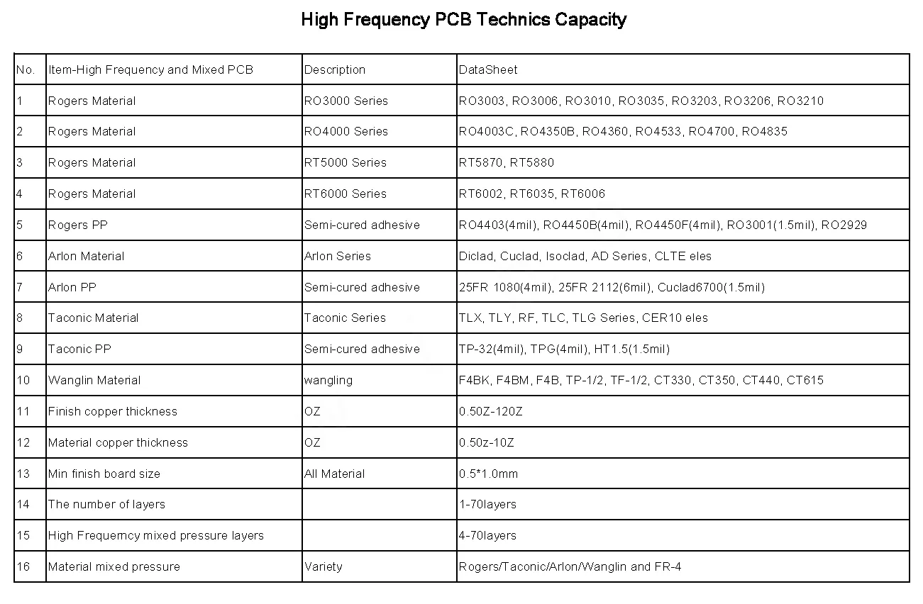
UGPCB is highly proficient in processing a wide range of premium high-frequency materials:
• Rogers RO4350B: Dk=3.48±0.05, Df=0,0037. Ideal for sub-6GHz 5G base station applications.
• Taconic RF-35: Dk=3.5±0.05, Df=0.0018. Suitable for millimeter-wave radar systems.
• PTFE (Polytétrafluoroéthylène): Dk=2.1-2.55, Df=0.0009. Optimized for 77GHz automotive radar.
• Isola I-Tera MT40: Dk=3.45±0.05, Df=0.0031. Excellent for high-speed backplane applications.
UGPCB also specializes in hybrid material lamination technology, effectively combining high-frequency materials with standard FR-4 to optimize cost-efficiency without compromising performance. Through precise control of lamination temperature (170°C±2°C) and pressure uniformity (erreur <3%), dielectric constant stability is enhanced to ±0.05, un 50% improvement over the industry average.
Precision Processing and Impedance Control Technology
Ultra-Fine Line Processing Capability
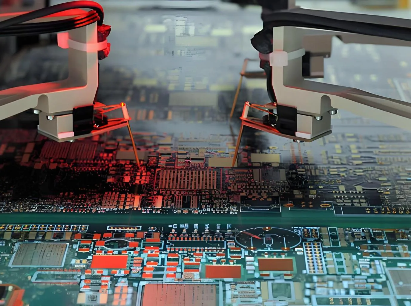
UGPCB possesses industry-leading circuit processing precision, achieving minimum trace width/space of 1.5mil/1.5mil (environ. 0.038mm), which is over six times finer than a human hair. By employing a composite “Laser Micro-etching + LDI Positioning” processus, trace edge roughness is controlled to Ra<0.5µm, un 40% improvement over traditional chemical etching.
Panneau multicouche layer-to-layer alignment error is maintained at <5µm, meeting the high-density routing requirements of 3-Step Sequential Lamination HDI PCB boards. This technology enhances PCB signal transmission efficiency by 8%, making it particularly suitable for interconnecting highly integrated chips.
Dynamic Impedance Compensation Technology
Contrôle d'impédance is the core of high-frequency PCB design. UGPCB utilizes fully automated CAM software for real-time trace correction, achieving a single-ended impedance tolerance of ±5Ω (compared to ±10Ω for standard boards) and a differential impedance tolerance of ±8Ω.
Precise calculation is performed using characteristic impedance formulas:
Microstrip Impedance Formula:
Z₀ = {87 / [sqrt(Ɛr + 1.41)]} * ln[5.98H / (0.8W + T)]
Where W is trace width, T is copper thickness, H is the distance to the reference plane, and Ɛr is the dielectric constant of the Substrat PCB.
Stripline Impedance Formula:
Z₀ = [60 / sqrt(Ɛr)] * ln{4H / [0.67π(T + 0.8W)]}
Where H is the distance between two reference planes, and the trace is centered between them.
Drilling and Hole Metallization Process
For high-frequency PCBs, UGPCB employs laser drilling technology to achieve microvia diameters of 0.1mm±0.02mm and hole position accuracy of ±25μm. Optimized drill wear control and deburring processes ensure minimal hole wall roughness, reducing conductor loss and signal reflection.
For hole copper thickness, high-frequency through-holes achieve ≥25μm (meeting Classe CIB 3 normes) with copper wall uniformity >85%, effectively preventing impedance discontinuities.
Multilayer Board Lamination and Reliability Assurance Process
Lamination Process Control
UGPCB holds unique advantages in multilayer board lamination. The process temperature is controlled 15-20°C below the substrate’s Tg to prevent material degradation; pressure uniformity across the panel is ≤7% deviation; and layer-to-layer alignment accuracy is ≤50μm.
Addressing the higher coefficient of thermal expansion (CTE) of high-frequency materials, temperature and pressure are strictly controlled during lamination to prevent warping and inner layer voids. Through brown oxidation treatment and optimization of multi-stage lamination parameters, the delamination rate has been reduced from 12% to below 3%.
Reliability Verification System
UGPCB implements military-grade reliability validation standards:
• Thermal Stress Test: 288° C, 10s for 5 cycles (pas de délaminage)
• TCD Test (Cyclisme thermique): -55°C to +125°C, 1000 cycles
• Humidity Testing: 85°C/85% RH for 48 heures, failure rate <0.01%
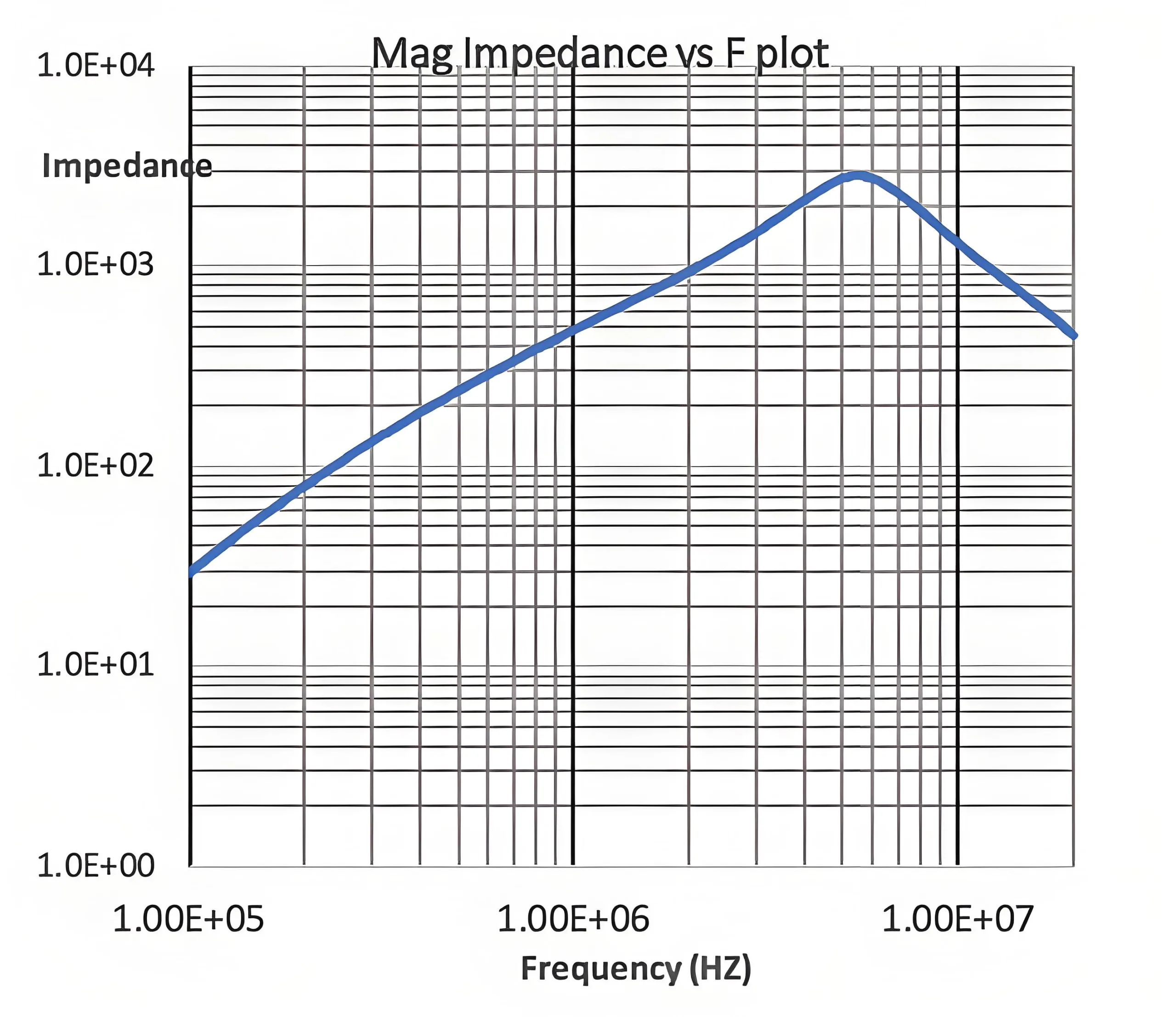
• High-Frequency Loss Testing: S-parameter measurement using a Vector Network Analyzer (VNA)
These rigorous tests ensure PCB performance remains uncompromised in extreme environments from -40°C to 150°C, meeting the reliability demands of military, automobile, et équipement médical.
Solutions for Specific Application Scenarios
5G Communication Equipment PCBs
UGPCB provides PCB solutions for 5G base station AAU antenna units and optical modules, supporting 28GHz high-frequency signals and 112Gbps high-speed interconnects. The use of blind and buried vias combined with impedance control technology ensures zero distortion for high-frequency signals.
A global top-3 communication equipment manufacturer utilized UGPCB’s 12-layer high-frequency PCB boards for a 5G base station project. The boards demonstrated signal loss below 0.3dB/inch and maintained stable transmission in extreme environments, helping the client’s product pass international certification and achieve mass production delivery.
Automotive Electronics Applications
To address heat dissipation and high-frequency signal attenuation in ADAS (Advanced Driver-Assistance Systems), UGPCB developed a 10-layer heavy copper PCB solution. Utilizing a 2mil/2mil ultra-fine line design with ENIG (Immersion Or) finition de surface, signal transmission loss was reduced by 40%. Combining high-frequency materials with a multi-layer grounding design elevated electromagnetic compatibility (CEM) to industry-leading levels.
The yield for a provided BMS (Système de gestion de batterie) mainboard increased from 92% à 98%, supporting 1000V high-voltage applications.
Medical and Military Applications
UGPCB’s high-frequency PCBs are used in CT scanner high-voltage circuit boards, complying with UL94-V0 flame retardancy standards. Optimization of image processing boards for 64-slice CT machines resulted in a 37% reduction in image noise.
For military radar applications, anti-jamming capabilities meet MIL-PRF-31032 standards. Using PTFE dielectric layers, signal loss is maintained below <0.5db, supporting 77GHz millimeter-wave automotive radar systems.
PCB Quality Control and Customer Value
Full-Process Quality Control System
UGPCB has established a digital inspection system:
• Online Inspection: Deployment of Zone d'intérêt (Inspection optique automatisée, 5Résolution μm) and AXI (Automated X-ray Inspection), achieving a defect recognition rate of 99.8% and a 20x efficiency increase over manual inspection.
• Offline Sampling: Utilization of 3D microscopes (0.1μm accuracy) and impedance testers (±3% tolerance), ensuring performance fluctuation of <5% per batch.
Through intelligent management of process parameters, UGPCB real-time monitors over 200 parameters (par ex., laser power, etch time). Dynamic threshold alerts trigger automatic machine adjustment for parameter deviations exceeding ±5%, increasing response speed by 10x compared to traditional manual checks.
Customer Value and Collaboration Benefits
UGPCB’s clientele includes a global top-3 communication equipment maker. The power amplifier module PCB for their 5G base station project, after optimization, achieved a 15% reduction in power consumption, helping the client complete mass production delivery 3 months ahead of schedule.
A drone manufacturer, after failures with three other suppliers, successfully resolved signal attenuation issues above 200MHz using UGPCB’s 10-layer 1st-order HDI PCB solution, enabling the project to move smoothly into mass production.
Conclusion
UGPCB has established itself as a leading provider of high-frequency PCB solutions through core strengths in material technology, precision processing, contrôle d'impédance, and reliability assurance. Through continuous innovation and a robust quality control system, UGPCB delivers high-performance, reliable high-frequency PCB products that drive technological progress in 5G communications, électronique automobile, dispositifs médicaux, and the military sector.
Avec plus 10 years of experience in high-precision PCB manufacturing, we can reduce time-to-market by 30%, from design review to mass production, providing customers with comprehensive technical support.
Industry experts and procurement professionals are welcome to inquire through our website. Our technical team is ready to provide you with professional high-frequency PCB and PCBA solutions.
WeChat
Scannez le code QR avec WeChat