
Introduction
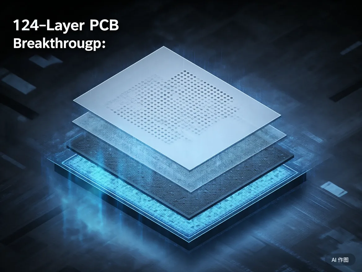
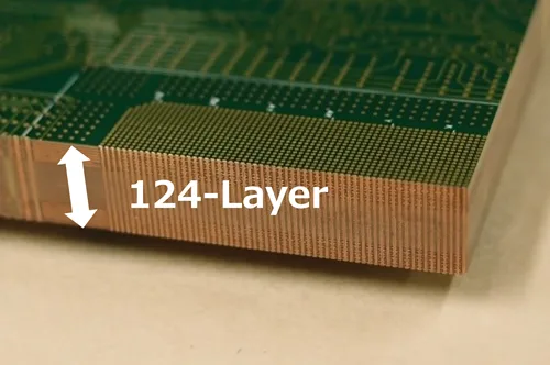
Prise par l'intelligence artificielle (IA) et l'informatique haute performance (HPC), L'industrie mondiale de l'électronique subit une révolution technologique centrée sur “densité élevée, grande vitesse, et une forte fiabilité.” En mai 2025, un leader Fabricant de PCB dévoilé la première carte de circuit imprimé commercial de 124 couches au monde, Briser la barrière de l'industrie de 108 couches de longue date tout en maintenant l'épaisseur standard de la planche de 7,6 mm. Ce jalon fournit non seulement une prise en charge matérielle critique pour les serveurs d'IA, tests de semi-conducteurs, et les systèmes de défense mais débloque également de nouvelles frontières dans la technologie d'emballage électronique.
Briser la barrière de 108 couches: Solutions d'ingénierie derrière les PCB de 124 couches
Innovations de fabrication de précision
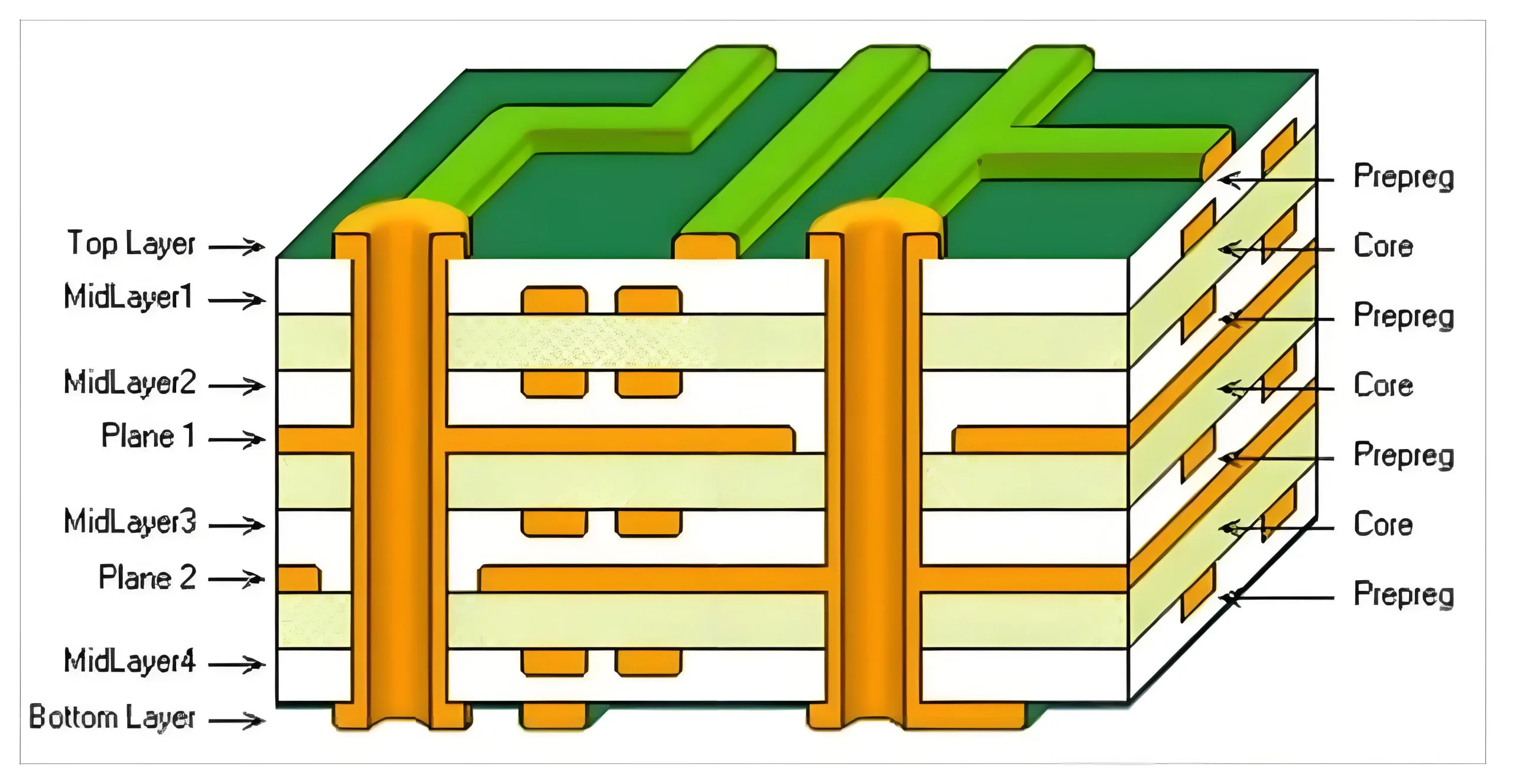
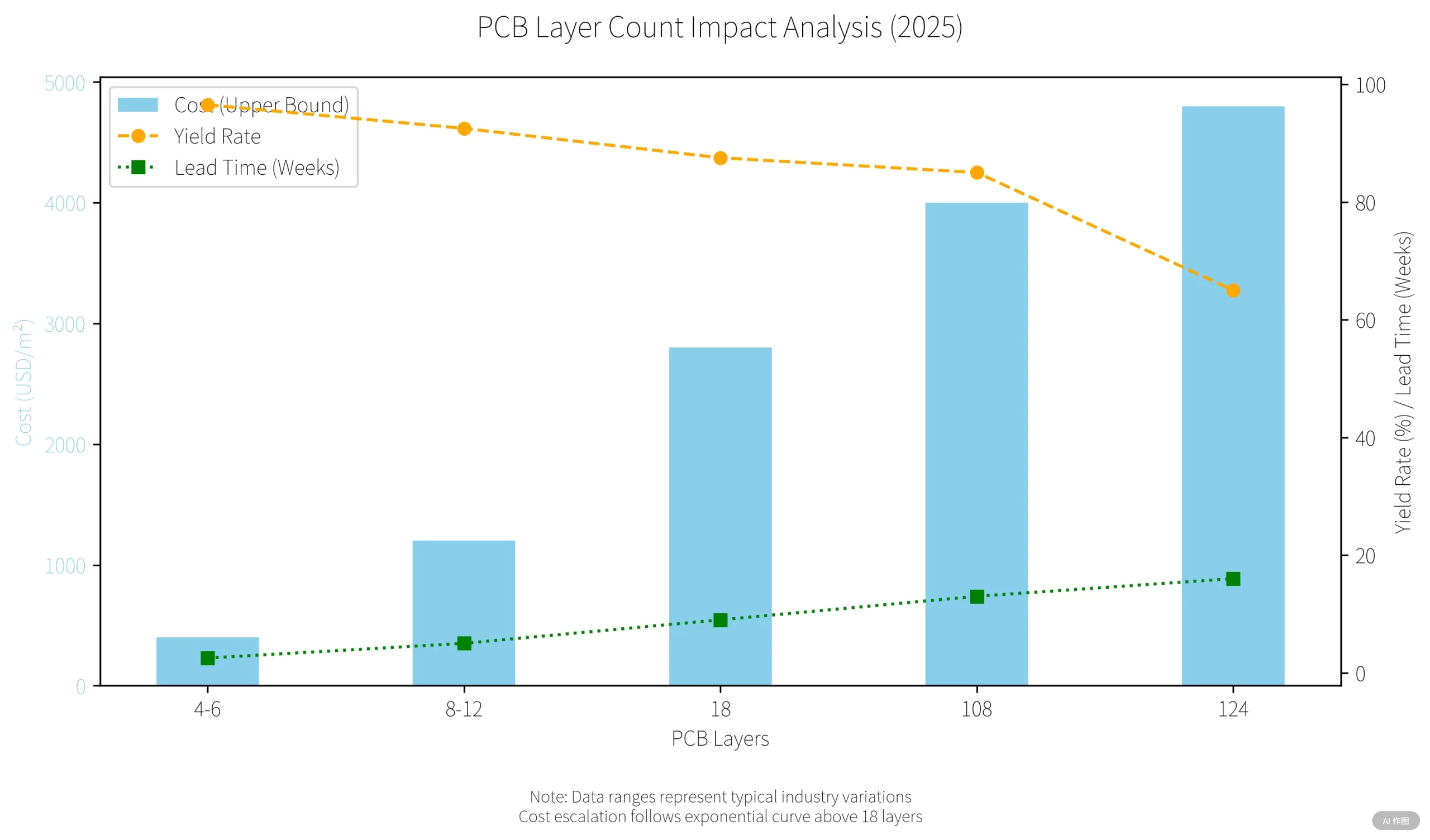
Traditionnel Conceptions de PCB Face Mechanical and Thermal Limitations à 100 couches dues aux incohérences de flux de résine, via l'effondrement, et le désalignement de la couche. Le PCB révolutionnaire 124 couches réalise un 15% Augmentation de la couche à travers:
-
Diélectriques ultra-minces: 25µm couches utilisant des matériaux à faible perte (par ex., Est tombé 7) avec ± 5% de contrôle d'impédance pour 112+ Signaux ghz
-
3D Optimisation d'interconnexion: Tableaux microvia permettant de 0,15 mm² / mm de densité de signal, conforme à PCIe Gen6 et CXL 3.0 protocoles
Certification de fiabilité thermique
Certifié selon les normes MIL-STD-883G, Le PCB de 124 couches résiste 1,000+ cycles thermiques (-55° C à 125 ° C) Tout en maintenant <1% perte de signal à 80 Stress mécanique MPA - ce qui le rend idéal pour les applications aérospatiales et de défense.
Applications: Accélérer les progrès matériels et semi-conducteurs
Serveurs d'IA & Mémoire à large bande passante (HBM)
-
Densité du signal: 18% Augmentation du routage des paires différentielles par couche
-
Gestion thermique: Les microvias remplis de cuivre améliorent la conductivité thermique par 30%, Critique pour les accélérateurs de 500W + AI
Tests de niveau à la plaquette & 3D Emballage
Permet la précision d'alignement submicron (± 0,8 mm) et contrôle de retard de signal de niveau Picoseconde pour les modules HBM empilés - un changeur de jeu pour les architectures basées sur Chiplet.
Défis de coût & Feuille de route d'évolutivité
Économie manufacturière
-
Coût matériel: 4,800/M2(contre.3,200/m² pour 108 couches)
-
Taux de rendement: 65% (16-cycle de la semaine) contre. 85% pour convention IDH
-
Analyse des échecs: Une coupe transversale destructrice requise pour 20% de défauts de contrainte thermique
Voies d'adoption industrielle
-
Fabrication additive: Réduit les pas de lament 40%
-
EDA dirigée par AI: Prédit via des points de stress avec 92% précision, potentiellement augmenter les rendements pour 75%
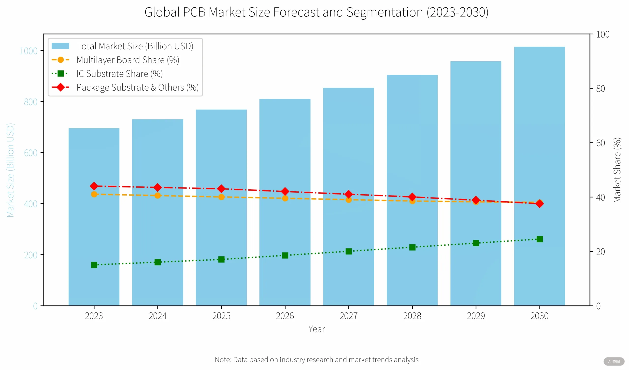
Perspectives du marché: $49B transformation de l'industrie B PCB
Moteurs de croissance
-
Cloud computing: 70% CAGR dans les PCB du serveur AI (CITIC SECURITIES 2026 projection)
-
Appareils AI Edge: 30% Augmentation des coûts de PCB dans les smartphones de nouvelle génération (Les données de la chaîne d'approvisionnement d'Apple)
-
Tendances de localisation: Les fabricants chinois aiment UGPCB ciblage de 3,6 m m² / an capacité de substrats avancés
Conclusion: Innovation pratique sur les enregistrements du nombre de couches
Tout en ne dépassant pas le prototype de 129 couches de Denso (2012), Ce PCB de 124 couches établit une nouvelle référence commerciale à travers:
-
Épaisseur standardisée (7.6mm) pour une compatibilité en arrière
-
Fiabilité mil-spec à 85% des coûts du prototype
-
Processus de fabrication évolutifs
À mesure que l'informatique quantique et la 6G émergent, L'innovation de PCB priorise la densité fonctionnelle sur le nombre de couches - un changement crucial pour les progrès technologiques durables.
