
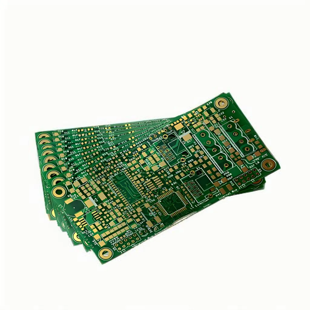
What is a 10Layers ENIG Board?
A 10-layer ENIG (Or par immersion au nickel autocatalytique) board is an advanced carte de circuit imprimé multicouche (PCB) with ten layers of conductive material, généralement en cuivre, séparés par des couches isolantes. Le “ACCEPTER” refers to the surface treatment applied to the copper traces, which involves electroless nickel and immersion gold plating. Ce type de PCB is designed for high-density and complex electronic applications.

Exigences de conception
Designing a 10-layer ENIG board involves several key considerations:
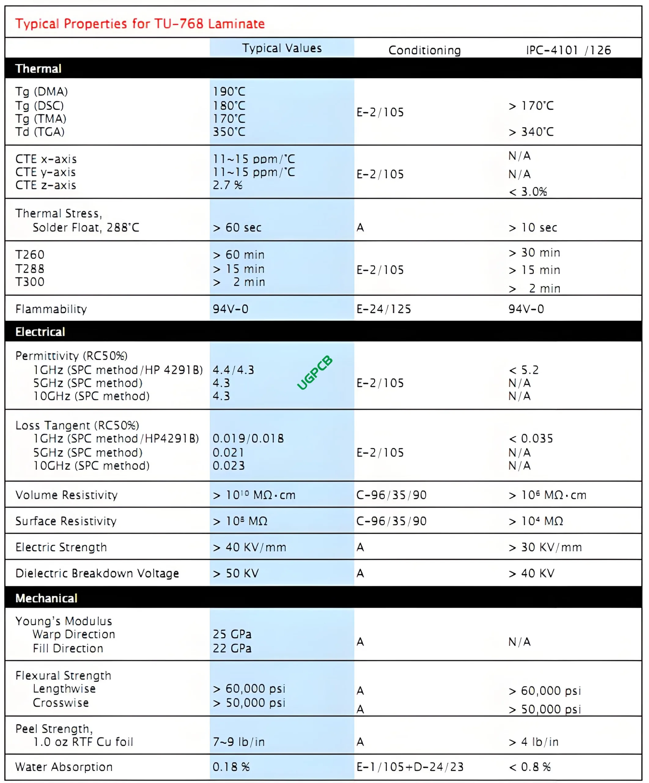
- Matériel: Fabriqué à partir de TU-768, a high-performance composite material known for its excellent electrical properties and durability.
- Nombre de couches: Consists of ten layers, allowing for intricate and dense circuit designs.
- Épaisseur du cuivre: Ranges from 2OZ to 3OZ, providing robust conductivity for high-power applications.
- Traitement de surface: Features immersion gold plating, which offers excellent solderability and corrosion resistance.
- Trace and Space: Minimum trace and space are set at 3mil (0.075mm), enabling fine details in the circuit design.
Comment ça marche?
The 10-layer ENIG board functions by providing multiple layers of conductive pathways, séparés par des couches isolantes, to interconnect electronic components. The immersion gold surface treatment ensures reliable soldering and long-term protection against oxidation and wear.
Applications

Due to their complexity and reliability, 10-layer ENIG boards are widely used in various high-end electronic applications including:
- Aerospace and defense systems
- High-speed networking equipment
- Advanced telecommunication devices
- Medical imaging equipment
Classification
10-layer ENIG boards can be classified based on several factors:
- Par matériau: Most commonly made from TU-768 due to its balance of cost, force, et propriétés électriques.
- By Copper Thickness: Varies from lightweight (2once) to heavyweight (3once) depending on the application’s needs.
- Par traitement de surface: Features immersion gold plating, which provides excellent solderability and corrosion resistance.
Matériaux utilisés
The primary materials used in manufacturing 10-layer ENIG boards include:
- TU-768: A glass-reinforced epoxy laminate that provides excellent mechanical strength and thermal stability.
- Cuivre: Used for the conductive layers, with thickness varying based on design requirements.
- Masque de soudure: Typically green or white, il protège les traces de cuivre de l'oxydation et des courts-circuits accidentels.
- Immersion Or: Applied as a surface treatment to improve solderability and protect against corrosion.
Caractéristiques de performance
Key performance attributes of a 10-layer ENIG board include:
- Densité élevée: Allows for more composants to be packed into a smaller area.
- Fiabilité: The use of multiple layers reduces the risk of electrical shorts and improves signal integrity.
- Intégrité du signal: Improved due to shorter signal paths and reduced crosstalk.
Composition structurelle
Structurellement, a 10-layer ENIG board comprises:
- Couches conductrices: Made of copper, etched into the desired circuit patterns.
- Couches isolantes: Éviter les courts-circuits électriques entre les couches conductrices.
- Plated Through-Hole Vias: Facilitate connections between different layers.
Caractéristiques distinctives
Some notable features of a 10-layer ENIG board are:
- Fine Pitch: Allows for high-density interconnects making it ideal for compact devices.
- Robustness: The use of multiple layers provides a strong mechanical bond between the board and components.
- Versatilité: Suitable for a wide range of applications due to customizable layer counts and material choices.
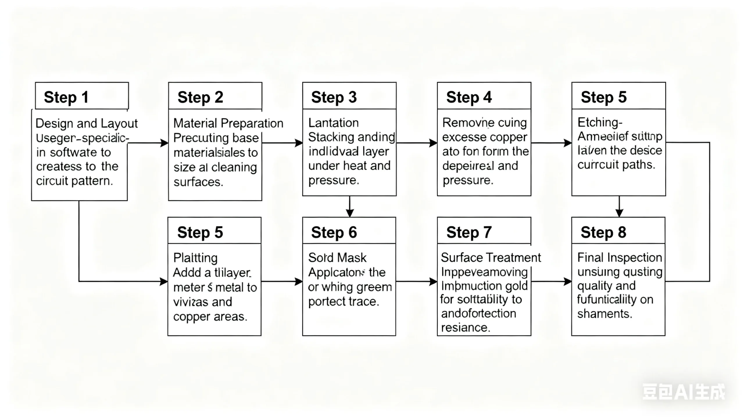
Processus de production
The manufacturing process of a 10-layer ENIG board involves several steps:
- Conception et disposition: Utiliser un logiciel spécialisé pour créer le modèle de circuit.
- Préparation des matériaux: Découpe des matériaux de base sur mesure et nettoyage des surfaces.
- Laminage: Empiler et coller des couches individuelles sous chaleur et pression.
- Gravure: Enlever l'excès de cuivre pour former les chemins de circuit souhaités.
- Placage: Ajout d'une fine couche de métal aux vias et aux zones de cuivre exposées.
- Application du masque de soudure: Applying the green or white coating to protect traces.
- Traitement de surface: Applying immersion gold for solderability and corrosion resistance.
- Inspection finale: Assurer la qualité et la fonctionnalité avant expédition.
Cas d'utilisation
Common scenarios where a 10-layer ENIG board might be employed include:
- High-density interconnect applications in aerospace and defense systems.
- Systèmes de communication avancés nécessitant une faible perte de signal.
- Instruments médicaux portables nécessitant des performances fiables dans des environnements difficiles.
- L’électronique automobile exigeant robustesse et longévité.
En résumé, the 10-layer ENIG board represents a significant advancement in printed circuit board technology offering unparalleled complexity and performance for modern electronic applications Its design flexibility combined with superior signal integrity and durability makes it an essential component in the development of next-generation high-end electronics and beyond


