Professional Product Overview
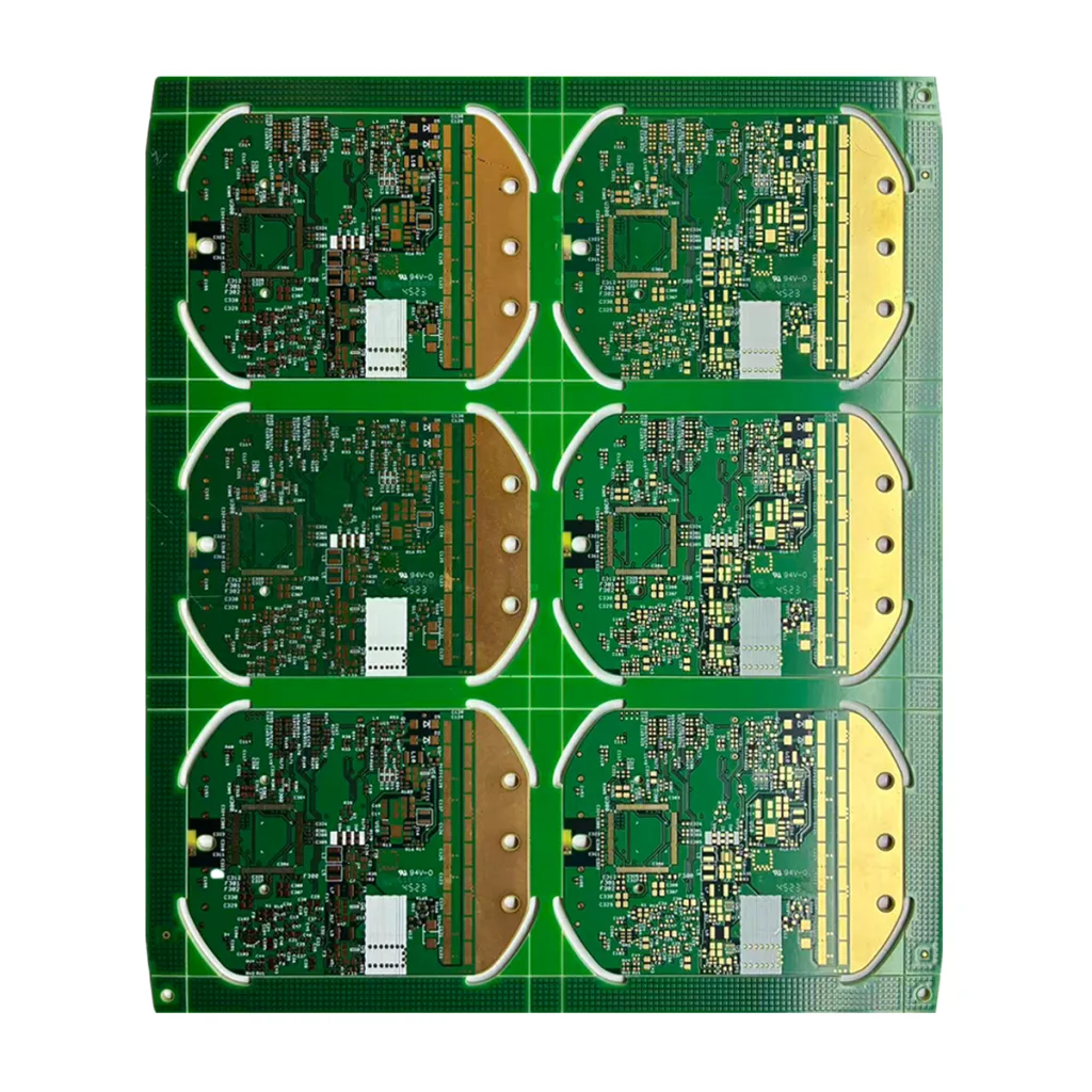
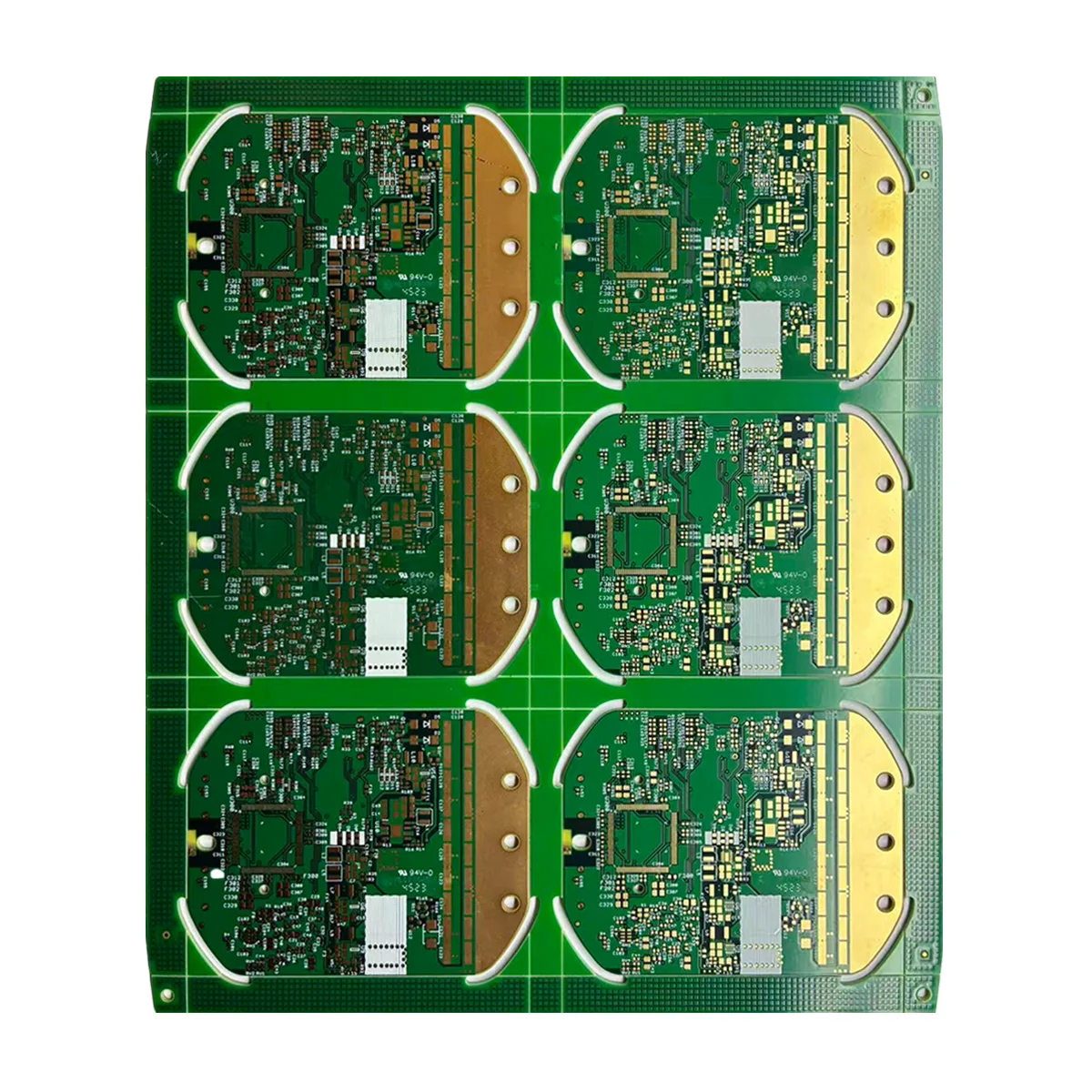
The UGPCB 12-Layer Rigid PCB is a high-end carte de circuit imprimé multicouche engineered for complex signal transmission, high-density interconnects (IDH), and demanding operating environments. Manufactured with high-performance FR-4 TU872SLK laminate and finished with 2-microinch Immersion Gold (ACCEPTER), this board is a cornerstone solution for industrial control systems, telecommunications infrastructure, and advanced computing hardware, offering exceptional electrical performance, long-term reliability, and robust signal integrity.
Définition du produit & Classification
This product is classified as a High-Layer Count Rigid Printed Circuit Board. It can be further categorized as:
-
Par structure: Rigide PCB.
-
Par nombre de couches: 12-Conseil multicouche de couche (mid-to-high layer count).
-
Par technologie: Standard Multilayer PCB suitable for complex, non-extreme miniaturization designs.
-
Par classe d'application: Industrial/Telecom-Grade PCB, meeting requirements for high reliability and long-term stability.
Considérations critiques de conception
Designing a 12-layer PCB requires meticulous attention to:
-
Stack-up Design: A rational stack-up sequence (par ex., alternating signal-ground-signal layers) is paramount for impedance control, crosstalk reduction, and Electromagnetic Compatibility (CEM). A proper 12-layer stack-up provides excellent power integrity and signal shielding.
-
Contrôle de l'impédance: Pour les signaux numériques à grande vitesse (par ex., DDR, Pie) or RF lines, precise calculation and control of trace characteristic impedance (par ex., 50Ω asymétrique, 90Ω/100Ω differential) are essential. We utilize advanced EDA tools and precise process controls to ensure consistency.
-
Pouvoir & Ground Plane Management: Solid ground planes and optimized power segmentation ensure low-noise power delivery and clear return paths, which are critical for system stability.
-
Gestion thermique: The 1.6mm board thickness and the thermal properties of FR-4 must align with component power dissipation. High-power areas may require thermal vias or integration with external cooling solutions.
Comment ça marche
A PCB is a passive platform that provides mechanical support, electrical interconnection, and signal transmission pathways for electronic components. This 12-layer PCB facilitates a complete working system by connecting chips, résistances, condensateurs, etc., through a complex network of etched copper traces. The multilayer architecture allows traces to cross on different layers without interference, significantly increasing circuit complexity and integration density. The ENIG surface finish guarantees reliable solder joints and long-term contact stability.
*(Suggestions d'images: Detailed cross-sectional diagram of a 12-layer PCB stack-up)*
*Alt Text: Cross-sectional view of a 12-layer PCB stack-up showing alternating copper layers and dielectric, illustrating complex internal structure for high-density interconnect.*
Construction & Matériels
-
Structure des couches: 12 conductive copper layers laminated with insulating prepreg.
-
Matériau de base: FR-4 TU872SLK. This is a high-performance epoxy glass laminate offering advantages over standard FR-4:
-
Higher Thermal Stability (Tg élevée, typically ≥170°C), providing better resistance to thermal expansion.
-
Superior Electrical Properties, with stable Dielectric Constant (Ne sait pas) et facteur de dissipation (Df) under high-temperature and high-frequency conditions.
-
Excellent CAF (Conductive Anodic Filament) Resistance, ideal for high-voltage, high-humidity environments, ensuring superior reliability.
-
-
Épaisseur finie: 1.60mm (nominal), with tight tolerance control (généralement ±10 %).
-
Finition de surface: Or par immersion au nickel autocatalytique (ACCEPTER). Épaisseur de nickel: 3-5µm; Épaisseur de l'or: 2 microinches (environ. 0.05µm). The gold layer protects the nickel from oxidation, providing a flat, surface soudable, while the nickel acts as a diffusion barrier between copper and gold.
Caractéristiques clés & Performance
-
Haute fiabilité: TU872SLK high-Tg material and ENIG finish ensure resistance to high temperatures, corrosion, and suitability for long-term operation in harsh environments.
-
Excellente intégrité du signal: Rigorous stack-up design and impedance control guarantee high-speed signal quality and lower bit error rates.
-
Strong Load-Bearing & Thermal Capacity: The 1.6mm thickness offers robust mechanical strength and substantial thermal load management.
-
Precision Solder Platform: The flat 2μ” ENIG surface is ideal for fine-pitch composants (par ex., Bgas), resulting in strong, reliable solder joints with low defect rates.
-
Interconnexion à haute densité (IDH): Twelve routing layers support complex, dense circuit designs, enabling reduced product footprint.
Flux de processus de fabrication
Inner Layer Imaging → AOI Inspection → Lamination & Pressing → Drilling → Electroless Copper Deposition → Outer Layer Imaging → Pattern Plating → Etching → Solder Mask Application → ENIG Surface Finish → Routing & Profiling → Electrical Testing → Final Quality Control (FQC)
Applications & Cas d'utilisation
This PCB is widely used in stability and performance-critical fields:
-
Automatisation industrielle: Contrôleurs API, servo drives, industrial robot control boards.
-
Équipement de télécommunications: Routeurs, commutateurs, base station cards, optical modules.
-
Électronique médicale: Control units for advanced medical imaging systems, moniteurs patients.
-
Test & Instruments de mesure: High-precision oscilloscopes, analyseurs de spectre, signal generators.
-
Pouvoir & Energy: Inverter control boards, Système de gestion de batterie (Bms) planches, smart meters.
-
Électronique automobile: High-end infotainment systems, Systèmes avancés d’aide à la conduite (Adas) domain controllers.