
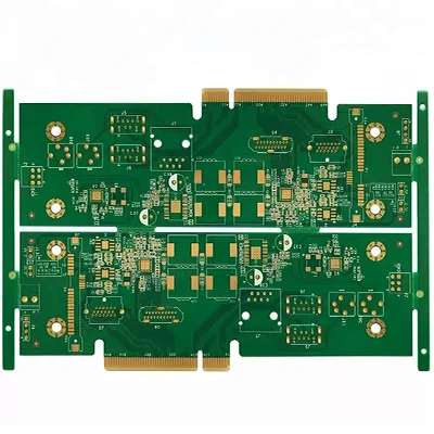
Overview of 6 Layer Golden Finger PCB
Le 6 Layer Golden Finger PCB is a high-precision, multi-layered printed circuit board designed for advanced electronic applications. This product combines multiple layers of conductive traces and insulating materials to provide exceptional performance and reliability in various electronic devices.
Définition
UN 6 Layer Golden Finger PCB is a type of multi-layer printed circuit board (PCB) that features six individual layers of conductive material, séparés par des couches isolantes. Le terme “Golden Finger” refers to the specific surface treatment applied to the edges of the board, which involves immersion gold and additional gold plating on the contact fingers.
Exigences de conception
When designing a 6 Layer Golden Finger PCB, several key requirements must be considered:
- Qualité des matériaux: High-quality FR4 material is essential for durability and performance.
- Configuration de la couche: Six layers are needed to accommodate complex circuitry and signal routing.
- Épaisseur du cuivre: A standard copper thickness of 1OZ ensures adequate conductivity.
- Traitement de surface: Immersion gold with additional gold finger plating enhances connectivity and corrosion resistance.
- Dimensions des traces/espaces: A minimum trace/space of 4mil/4mil is required for precise circuit patterns.
- Processus spéciaux: The gold finger process with a thickness of 0.1um is critical for reliable edge connections.
Principe de fonctionnement
Le 6 Layer Golden Finger PCB operates based on the principles of electrical conductivity and insulation. Conductive traces on different layers create pathways for electrical signals, tandis que les couches isolantes empêchent les interactions indésirables entre ces signaux. The gold finger edges facilitate easy insertion into connectors, ensuring stable and reliable connections.
Applications
This type of PCB is widely used in applications that require high precision and reliability, tel que:
- High-speed digital circuits
- Équipement de télécommunications
- Advanced computing systems
- Électronique automobile
- Dispositifs médicaux
Classification
6 Layer Golden Finger PCBs can be classified based on their intended use, tel que:
- Cartes de traitement du signal: Pour gérer les signaux de haute fréquence dans les appareils de communication.
- Cartes de distribution d'électricité: Pour gérer l'alimentation dans les systèmes électroniques complexes.
- Tableaux de contrôle: For controlling and managing various functions in electronic devices.
Matériels
Les matériaux principaux utilisés dans la construction d'un 6 Layer Golden Finger PCB include:
- Matériau de base: FR4, un matériau en fibre de verre ignifuge connu pour ses excellentes propriétés diélectriques et sa résistance mécanique.
- Matériau conducteur: Cuivre, utilisé pour les traces conductrices.
- Traitement de surface: Immersion gold and additional gold plating for the gold fingers.
Performance
La performance d'un 6 Layer Golden Finger PCB is characterized by:
- Intégrité élevée du signal: Grâce à des dimensions de trace/espace précises et à des matériaux de qualité.
- Connectivité fiable: Ensured by the gold finger surface treatment.
- Durabilité: Enhanced by the robust FR4 base material and immersion gold finish.
- Efficacité électrique: Perte de signal et interférences minimisées grâce à une configuration de couche optimisée.
Structure
La structure d'un 6 Layer Golden Finger PCB consists of:
- Six couches de matériau conducteur: En alternance avec des couches isolantes.
- Gold Finger Edges: Plated with a thin layer of gold for enhanced connectivity.
- Protective Layers: Including solder mask and silkscreen for protection and identification.
Caractéristiques
Key features of the 6 Layer Golden Finger PCB include:
- Traitement de surface avancé: Immersion gold plus gold finger for superior connection quality.
- Haute précision: With a minimum trace/space of 4mil/4mil.
- Options de couleurs personnalisables: Disponible en vert ou blanc.
- Épaisseur standard: Avec une épaisseur finie de 1,6 mm.
Processus de production
The production process for a 6 Layer Golden Finger PCB involves several steps:
- Préparation des matériaux: Sélection et préparation des feuilles FR4 et des feuilles de cuivre.
- Empilement de calques: Alternance de couches de cuivre et de matériaux isolants.
- Gravure: Retirer l'excès de cuivre pour former le motif de circuit souhaité.
- Placage: Applying immersion gold and additional gold finger plating.
- Laminage: Combiner les couches sous chaleur et pression.
- Forage: Création de trous pour les composants à travers et les vias.
- Application du masque de soudure: Protéger le circuit des ponts de soudure et des facteurs environnementaux.
- Sérigraphie: Ajout de texte et de symboles pour le placement et l'identification des composants.
- Contrôle de qualité: Assurer que le PCB répond à toutes les spécifications et normes de conception.
Utiliser des scénarios
Le 6 Layer Golden Finger PCB is ideal for scenarios where:
- Une intégrité élevée du signal est cruciale.
- Des connexions fiables et durables sont nécessaires.
- Les contraintes d'espace nécessitent une conception compacte et efficace.
- Un traitement de surface avancé est nécessaire pour des performances améliorées.


