Introduction to Optical Module HDI PCB by UGPCB
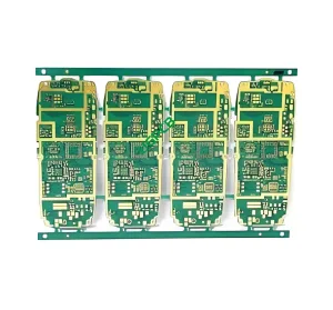
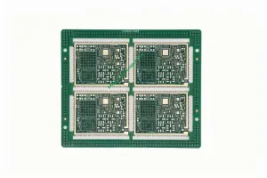
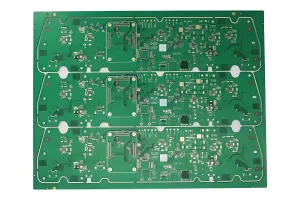
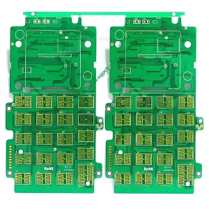
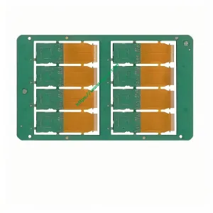
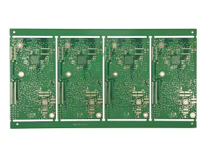
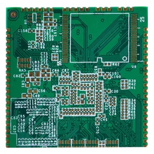
UGPCB’s Optical Module HDI PCB represents the pinnacle of high-density interconnect technology, engineered specifically for the demanding requirements of modern optical communication systems. This 8-layer board, constructed with premium TG170 FR4 material and a sophisticated 2+4+2 IDH build, is designed to facilitate ultra-high-speed data transmission with exceptional signal integrity and reliability. As a critical component in optical transceivers, ce PCB exemplifies advanced manufacturing capabilities, including 3mil trace/space and electric hard gold surface treatment, making it a cornerstone of next-generation networking infrastructure.

Product Definition and Overview
An Optical Module HDI PCB is a specialized high-density interconnect printed circuit board that serves as the fundamental platform for optical transceiver modules. These modules are essential for converting electrical signals into optical signals and vice versa, forming the backbone of high-speed data communication networks. UGPCB’s version is an 8-layer marvel with a finished thickness of just 0.8mm, utilizing a 2+4+2 HDI construction. This design incorporates multiple layers of microvias and buried vias to achieve a higher wiring density than conventional PCBs, which is paramount for the compact form factors and high-speed performance required in optical applications.
Key Design Considerations for High-Frequency PCBs
The design of an HDI PCB for optical modules requires meticulous attention to several critical factors. Signal integrity is paramount; impedance control must be precisely managed throughout the board to prevent signal degradation at high frequencies. The minimal trace and space of 3mil/3mil demand advanced design rules and manufacturing precision. Power integrity is another crucial aspect, ensuring stable voltage delivery to sensitive components. En outre, thermal management is integrated into the design to dissipate heat effectively, maintaining performance and longevity. These design considerations are vital for producing a reliable PCB for high-speed applications.
How an Optical Module PCB Operates
The core function of this PCB is to provide a stable and efficient electrical pathway between the laser driver, the photodiode, and the host system. Electrical signals from the host system are processed by integrated circuits on the board and directed to a laser driver, which modulates a laser diode to produce light pulses. Conversely, incoming light pulses are received by a photodetector, converted back into electrical signals, and amplified before being sent to the host. The HDI PCB’s design ensures these high-speed signals travel with minimal loss, distorsion, or crosstalk, enabling reliable data transmission.
Primary Applications and Use Cases
The primary application of this advanced PCB HDI is within optical transceiver modules used in data centers, telecommunications infrastructure, and high-performance computing clusters. These modules, and by extension the PCBs, are found in switches, routeurs, and servers, enabling high-speed fiber optic communication links such as 400G and 800G Ethernet. Their use is critical in scenarios demanding immense bandwidth and low latency, including cloud computing, big data analytics, and 5G network backhaul.
Classification of HDI PCBs
HDI PCBs are classified based on their construction complexity, often denoted by a sequence of numbers (par ex., 2+4+2). This indicates the build-up layers on each side of the core. UN 2+4+2 PCB HDI, like the one from UGPCB, features two sequential build-up layers on both sides of a four-layer core. This classification signifies a high tier of complexity, allowing for a greater density of components and interconnections compared to simpler 1+N+1 constructions.
Materials and Composition: TG170FR4
The choice of matériel is critical for performance. UGPCB uses TG170 FR4, a high-performance laminate. Le “TG170” denotes a glass transition temperature of 170°C, meaning the material remains stable and maintains its mechanical properties under high thermal stress, which is common during assembly and operation. This FR4 variant offers excellent electrical insulation, résistance mécanique, et fiabilité, making it an ideal substrate for demanding HDI PCB manufacturing.
Performance Characteristics and Specifications
This Optical Module HDI PCB is defined by its exceptional performance specs:
-
Intégrité du signal: Excellent dielectric properties and controlled impedance for multi-gigabit data rates.
-
Fiabilité thermique: High Tg material ensures stability during lead-free (RoHS) Assemblage PCBAy processes.
-
Durabilité: Electric hard gold plating, particularly on the golden finger beveled edge, provides superior wear resistance for repeated mating cycles.
-
Précision: 3mil line width and spacing allow for complex routing in a compact space.
-
Profil: Ultra-thin 0.8mm profile fits standard optical module housings.
Detailed Board Structure: 2+4+2 HDI Build
Le 2+4+2 structure is a key feature. It starts with a traditional 4-layer core. Two additional HDI build-up layers are added on each side of this core. These build-up layers are connected using microvias (laser-drilled holes) that only pass through one layer at a time, allowing for much denser routing. This structure enables the placement of fine-pitch BGA components and the complex routing necessary for high-speed differential pairs, all within a very thin overall board profile.
Distinguishing Features and Advantages
UGPCB’s Optical Module HDI PCB offers several distinct advantages:
-
Conception à haute densité: Maximizes functionality in a minimal space.
-
Enhanced Signal Performance: Optimized layer stackup and materials minimize signal loss.
-
Superior Surface Finish: Electric hard gold offers excellent conductivity and corrosion resistance.
-
Construction robuste: High Tg material ensures reliability under thermal and mechanical stress.
-
Beveled Golden Fingers: Precise beveling ensures smooth insertion and connection reliability.
The HDI PCB Manufacturing Process Flow
The production of this PCB involves a sophisticated multi-step process: 1) Laser drilling of microvias on the inner layers; 2) Sequential lamination of the core and build-up layers; 3) Electrolytic copper deposition to plate the vias; 4) Advanced imaging and etching to achieve 3mil traces; 5) Application of electric hard gold plating, including selective plating on the golden fingers; 6) Precise beveling of the edge connector; 7) Electrical testing and final inspection to ensure 100% fonctionnalité.
Conclusion: Ideal Usage Environments

This high-performance Optical Module HDI PCB from UGPCB is specifically engineered for deployment in environments where reliability, vitesse, and density are non-negotiable. Its primary use case is within data centers and networking hubs that form the core of global digital communication. It is the ideal solution for OEMs and designers who require a trusted PCB and PCB partner capable of delivering boards that meet the extreme demands of cutting-edge optical communication technology.
 LOGO UGPCB


