

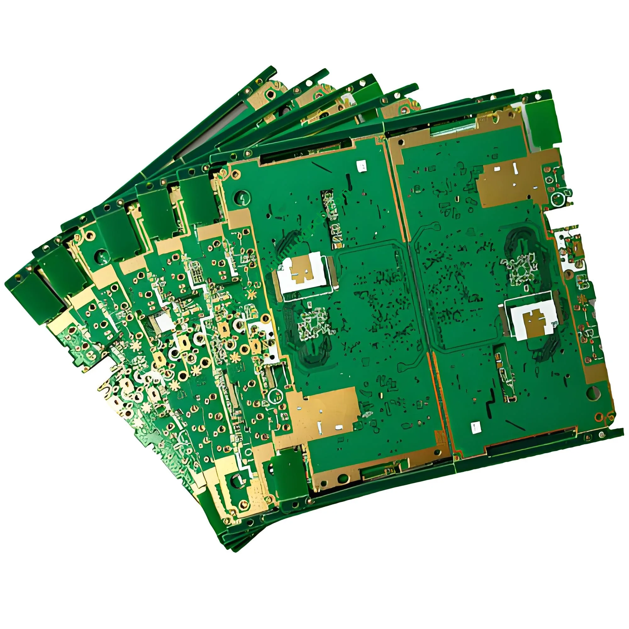
나. 제품개요: A PCB Board Engineered for Wireless Doorbell Systems
The wireless doorbell PCB circuit board is an essential electronic component in smart home and security systems. UGPCB offers this board built with Kingboard KB6165F high-performance copper-clad laminate. The manufacturing process follows strict quality controls.
This wireless doorbell PCB is a 2-layer double-sided 인쇄 회로 기판. It has a 1.0mm thickness and measures 79.48 × 35.6mm. These dimensions fit perfectly into compact wireless doorbell enclosures. The board uses a lead-free HASL (열기 솔더 레벨링) 표면 마감. This finish meets RoHS environmental requirements while delivering excellent solderability.
Wireless doorbells serve as the first line of defense in home security. The reliability of their circuit boards directly determines product lifespan and user experience. UGPCB understands this critical requirement. We carefully select materials and control every process step to deliver high-quality wireless doorbell PCB 보드 to customers worldwide.
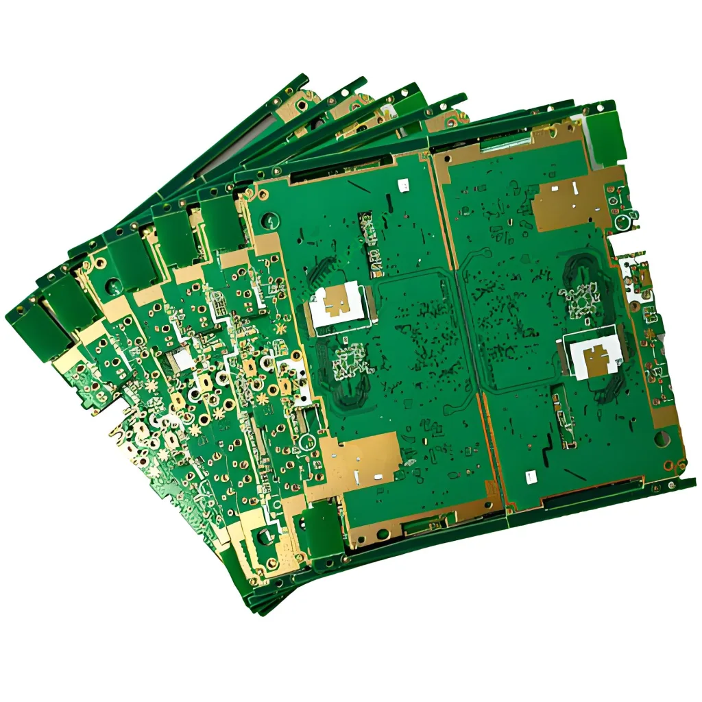
II. Product Definition and Industry Positioning
에이wireless doorbell PCB circuit board is a printed circuit board used in wireless doorbell systems. It typically consists of two parts: a transmitter board and a receiver board. The transmitter PCB carries the encoder chip (HT12E와 같은), a 433MHz wireless transmitter module, and the push-button switch circuit. The receiver PCB carries the decoder chip (HT12D와 같은), the wireless receiver module, the audio amplifier, and the speaker driver circuit.
PCB 분류 관점에서, 이 제품은rigid double-sided printed circuit board (견고한 양면 PCB) . It can be further classified as follows:
| 분류 차원 | 범주 |
|---|---|
| 전도성 층 | 양면 (2엘) |
| Substrate Rigidity | 리지드 보드 |
| 표면 마감 | 무연 HASL |
| 가연성 등급 | UL 94 다섯-0 |
| IPC 성능 등급 | 수업 2 (전용 서비스 전자 제품) |
This product complies with IPC-6012경질 인쇄 기판의 자격 및 성능 사양. Its substrate material, KB6165F, meets the IPC-4101/99 specification requirements.
III. 주요 기술 매개변수
3.1 기판 재료: Kingboard KB6165F Copper-Clad Laminate
KB6165F는lead-free Tg150 glass fabric copper-clad laminate manufactured by Kingboard Laminates Holdings Limited. It belongs to the FR-4 grade epoxy glass fabric laminate family. The key performance indicators are as follows:
- 유리전이온도 (Tg) : 154℃ (테스트 방법: IPC-TM-650 2.4.25)
- z 축 Cte (열 팽창 계수) : 40 ppm/°C (50-260°C), total expansion 3.1% (테스트 방법: IPC-TM-650 2.4.24)
- T-288 Delamination Time : >30 분 (테스트 방법: IPC-TM-650 2.4.24.1)
- 열분해 온도 (Td, 5% 체중 감량) : 346℃ (테스트 방법: IPC-TM-650 2.4.24.6)
- 가연성 등급 : UL 94 다섯-0
- 유전 상수 (DK) @ 1GHz : 4.6 (테스트 방법: IPC-TM-650 2.5.5.2)
- 소산 인자 (Df) @ 1GHz : 0.016 (테스트 방법: IPC-TM-650 2.5.5.2)
- 껍질 힘 (1 온스 구리 호일) : 1.4 N/mm (테스트 방법: IPC-TM-650 2.4.8)
- 굽힘 강도 : 550 N/mm² (longitudinal) / 485 N/mm² (transverse) (테스트 방법: IPC-TM-650 2.4.4)
- 수분 흡수 : 0.10% (테스트 방법: IPC-TM-650 2.6.2.1)
- 열 응력 : ≥240 seconds (테스트 방법: IPC-TM-650 2.4.13.1)
A high Tg (>150℃) means this substrate can withstand the high temperatures of lead-free soldering processes. It effectively prevents board warping and delamination during assembly. Its excellent anti-CAF (전도성 양극 필라멘트) performance ensures reliability in humid environments and under long-term power-on conditions.
3.2 보드 두께 및 레이어 수
보드 두께는1.0mm ~와 함께2 레이어 (2엘) . This thickness provides sufficient mechanical strength while supporting the thin and compact design requirements of wireless doorbell products. The double-layer design allows proper layout of RF circuits, power circuits, and control circuits on both the transmitter and receiver boards. This optimizes signal integrity and power integrity.
3.3 치수
The dimensions are79.48mm × 35.6mm. This compact size is optimized for the internal space of wireless doorbell products. It accommodates all functional circuits while fitting easily into various doorbell enclosures.
3.4 최소 조리개
The minimum aperture is0.332mm. According to IPC-6012 requirements for plated-through holes, this aperture size meets the reliability needs of component lead insertion and via metallization in wireless doorbell PCB boards.
3.5 추적 너비와 간격
The trace width is0.42mm and the trace spacing is0.46mm. IPC-2221에 따르면인쇄 기판 설계에 대한 일반 표준, the current-carrying capacity can be calculated using the following formula:
어디:
- = 최대 전류 전달 용량 (amperes)
- = 보정 계수 (0.048 외부 레이어용, 0.024 내부 레이어용)
- = 허용 온도 상승 (℃)
- = 도체 단면적 (제곱밀)
외부 레이어 트레이스의 경우 1 온스 구리 호일 (1.37 mils thick) and a trace width of 0.42mm (약 16.5 밀), the cross-sectional area is:
10°C 온도 상승 시, the theoretical current-carrying capacity is:
This current capacity fully meets the requirements of low-power RF circuits and digital control circuits in wireless doorbell PCB boards.
3.6 동박 두께
The copper foil thickness is1/1온스 (1 양쪽 외층 모두 oz, 약 35μm). This thickness provides an excellent balance between current-carrying capacity, 열전도도, 그리고 비용. It is the standard configuration for consumer electronics PCBs.
3.7 표면 마감: 무연 HASL
표면 마감은무연 HASL (열기 솔더 레벨링) . 이 과정에서, the PCB is immersed in molten lead-free solder alloy (typically Sn99.3Cu0.6). High-pressure hot air knives then blow across the surface to remove excess solder.
The key advantages of lead-free HASL surface finish include:
- 우수한 납땜성 : Suitable for multiple soldering cycles
- 긴 유통기한 : The solder alloy provides good storage stability
- 비용 효율성 : More economical than ENIG and other finishes
- RoHS 준수 : Contains no lead or other restricted substances
This surface finish meets the coating requirements specified in IPC-6012.
3.8 솔더 마스크 및 범례
The solder mask is녹색 잉크 and the legend is흰색 잉크. Green solder mask is the most popular choice in the PCB industry. It offers excellent insulation properties, 내열, and visual clarity. White legend ensures that component designators, 극성 표시, and other information remain clearly readable.
IV. Design Guidelines and Operating Principles
4.1 설계 지침
Wireless doorbell PCB 설계 requires attention to several critical areas:
(1) RF Circuit Design
Wireless doorbells typically operate in the 433MHz ISM band. RF traces must be designed as 50Ω characteristic impedance microstrip lines or coplanar waveguides. The trace width must be precisely calculated based on the PCB 재료 매개변수 (dk = 4.6). The antenna should be placed near the PCB edge. Avoid placing it in the middle of the board or surrounding it with large ground planes.
(2) 전력 무결성
The power management circuits on both transmitter and receiver boards require proper layout. Place decoupling capacitors close to IC pins following the “near and multiple” 원칙.
(3) Interference Mitigation
Place the receiver circuit in a corner of the PCB, away from switching power supplies and other noise sources. The crystal oscillator circuit needs its own ground plane and should be placed as close to the MCU as possible.
(4) 열 관리
The 1.0mm board thickness combined with 1 oz copper foil provides good thermal conductivity. This effectively dissipates heat from RF power amplifiers and other heat-generating components.
4.2 작동 원리
A wireless doorbell system consists of a transmitter and a receiver:
Transmitter Operation : When a user presses the doorbell button, the encoder chip (HT12E와 같은) on the transmitter PCB encodes the button signal. The 433MHz RF transmitter module then sends this encoded signal wirelessly. The transmitter typically draws about 5.6mA during operation.
Receiver Operation : The 433MHz RF receiver module on the receiver PCB continuously monitors for wireless signals. When it receives a matching encoded signal, the decoder chip (HT12D와 같은) decodes it. This triggers the audio amplifier circuit to drive the speaker and produce the doorbell chime.
다섯. Product Features and Performance Advantages
5.1 제품 기능
| 특징 | 설명 |
|---|---|
| High-Reliability Substrate | Kingboard KB6165F Tg150 laminate, UL 94 다섯-0 flame retardant |
| Environmentally Friendly Lead-Free Process | Lead-free HASL surface finish, ROHS 준수 |
| 정밀 제조 역량 | 최소 조리개 0.332mm, supports high-density routing |
| Excellent Heat Resistance | T-288 >30분, withstands lead-free reflow soldering temperatures |
| 우수한 전기적 성능 | Dk=4.6, Df=0.016 @ 1GHz, suitable for RF applications |
| High Dimensional Accuracy | Precise 79.48×35.6mm dimensions, fits standard doorbell housings |
5.2 성능상의 이점
(1) 국제 표준 준수
The product is designed and manufactured in compliance with IPC-6012경질 인쇄 기판의 자격 및 성능 사양 및 IPC-A-600인쇄 기판의 수용성. The substrate meets IPC-4101/99 specification requirements.
(2) UL 안전 인증
KB6165F substrate has obtained UL certification (UL File No. E123995). Its flame retardancy rating meets UL 94 다섯-0. It also complies with UL 796인쇄 배선 기판 표준 for rigid boards used as components in devices or appliances.
(3) Environmental Robustness
The low Z-axis CTE (40 ppm/°C) and excellent anti-CAF performance ensure long-term reliability under temperature cycling and humid conditions.
VI. 제조 공정 흐름
UGPCB follows a standardized manufacturing process for wireless doorbell PCB boards:
① 입고자재 검사 → Inspect substrate and copper foil per IPC-A-600
② Inner Layer Circuit Formation → 라미네이트 드라이 필름, 폭로하다, 개발하다, and etch to form inner layer circuit patterns
③ 라미네이션 → Laminate inner layer cores with prepreg (PP) under high temperature and pressure
④ 드릴링 → CNC 교련, minimum aperture 0.332mm
⑤ 무전해 동증착 / 패널 도금 → Electroless copper deposition + full-board electroplating for interlayer electrical connection
⑥ Outer Layer Circuit Formation → Laminate film, 폭로하다, 개발하다, pattern plate, and etch to form outer layer circuits
⑦ Solder Mask Application → Apply green solder mask ink to protect circuits and prevent soldering shorts
⑧ Surface Finish → Lead-free HASL (열기 솔더 레벨링)
⑨ Legend Printing → Print white legend to identify component designators
⑩ 라우팅 → CNC routing or punching to final 79.48×35.6mm dimensions
⑪ Electrical Testing → 플라잉 프로브 or fixture testing for 100% open/short detection
⑫ 최종검사 → Visual and dimensional inspection per IPC-A-600
⑬ Packaging and Shipping → Vacuum packaging with moisture protection
Ⅶ. Application Scenarios and End-Use Markets
Wireless doorbell PCB boards are widely used in the following applications:
| 응용 시나리오 | 설명 |
|---|---|
| Residential Wireless Doorbells | Home entry doorbell systems with transmitter outdoors and receiver indoors |
| Smart Building Intercoms | Wireless call units for apartment building access systems |
| Hotel Service Call Systems | Wireless transmitter modules for hotel room service call buttons |
| Elderly Care Emergency Call Systems | Wireless transmitter PCBs for senior emergency help buttons |
| Smart Home IoT Devices | Smart doorbells with integrated Wi-Fi modules |
| Security and Surveillance Systems | Wireless trigger and alarm units for security equipment |
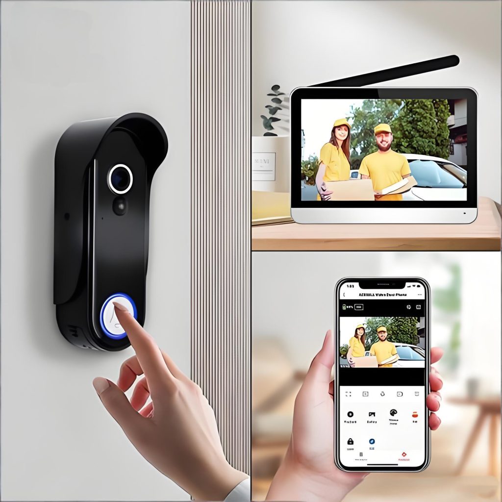
Wireless doorbell PCB boards are core components in consumer electronics and smart home devices. Market demand continues to grow. As smart home adoption accelerates, the need for high-quality, high-reliability wireless doorbell PCB boards is increasing rapidly.
Ⅷ. Why Choose UGPCB Wireless Doorbell PCB Boards?
✅ Premium Substrate Material : Kingboard KB6165F Tg150 laminate with UL 94 다섯-0 flame retardancy ensures product safety and reliability
✅ 국제 표준 준수 : Design and manufacturing comply with IPC-6012, IPC-A-600, IPC-2221, and other international specifications
✅ Environmentally Friendly Lead-Free Process : Lead-free HASL surface finish meets RoHS environmental requirements
✅ Precision Manufacturing Capability : 최소 조리개 0.332mm, trace width/spacing 0.42/0.46mm for high-precision routing needs
✅ Professional RF Design Support : 50Ω impedance control and other professional design support for 433MHz wireless doorbell applications
✅ Fast Delivery : Prototypes in 4–5 days with expedited options available
9. Inquiry and Ordering Guide
UGPCB is committed to providing high-quality wireless doorbell PCB boards and PCB turnkey services to customers worldwide. Whether you are a hardware engineer developing a new wireless doorbell product or a procurement manager seeking a reliable PCB supplier, UGPCB는 귀하의 신뢰할 수 있는 파트너입니다..
Request a quote today to receive exclusive pricing and dedicated technical support.
📧이메일 : info@ugpcb.com
🌐웹사이트 : www.ugpcb.com
Please provide your PCB design files (거버 파일), 자료 청구서 (BOM), and any special process requirements. The UGPCB professional team will respond within 24 hours with an optimized PCB/PCBA solution.
데이터 소스 선언
The technical data cited in this document are sourced from the following authoritative organizations and standards:
- Kingboard Laminates Holdings Limited : KB-6165F Copper-Clad Laminate Technical Data Sheet
- IPC — 전자 산업 연결 협회 : IPC-6012 경질 인쇄 기판의 자격 및 성능 사양
- IPC — 전자 산업 연결 협회 : IPC-A-600 인쇄 기판의 수용성
- IPC — 전자 산업 연결 협회 : IPC-2221 인쇄 기판 설계에 대한 일반 표준
- IPC — 전자 산업 연결 협회 : IPC-TM-650 테스트 방법 매뉴얼 (2.4.4, 2.4.8, 2.4.13.1, 2.4.24, 2.4.24.1, 2.4.24.6, 2.4.25, 2.5.5.2, 2.6.2.1)
- UL — 보험업자 연구소 : UL 796 인쇄 배선 기판 표준
- UL — 보험업자 연구소 : UL 94 기기 및 가전제품 부품용 플라스틱 재료의 난연성 시험에 대한 표준













