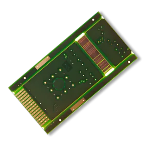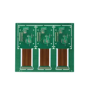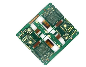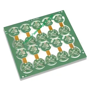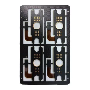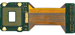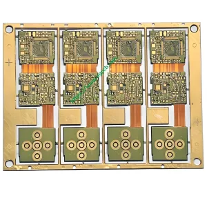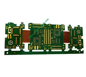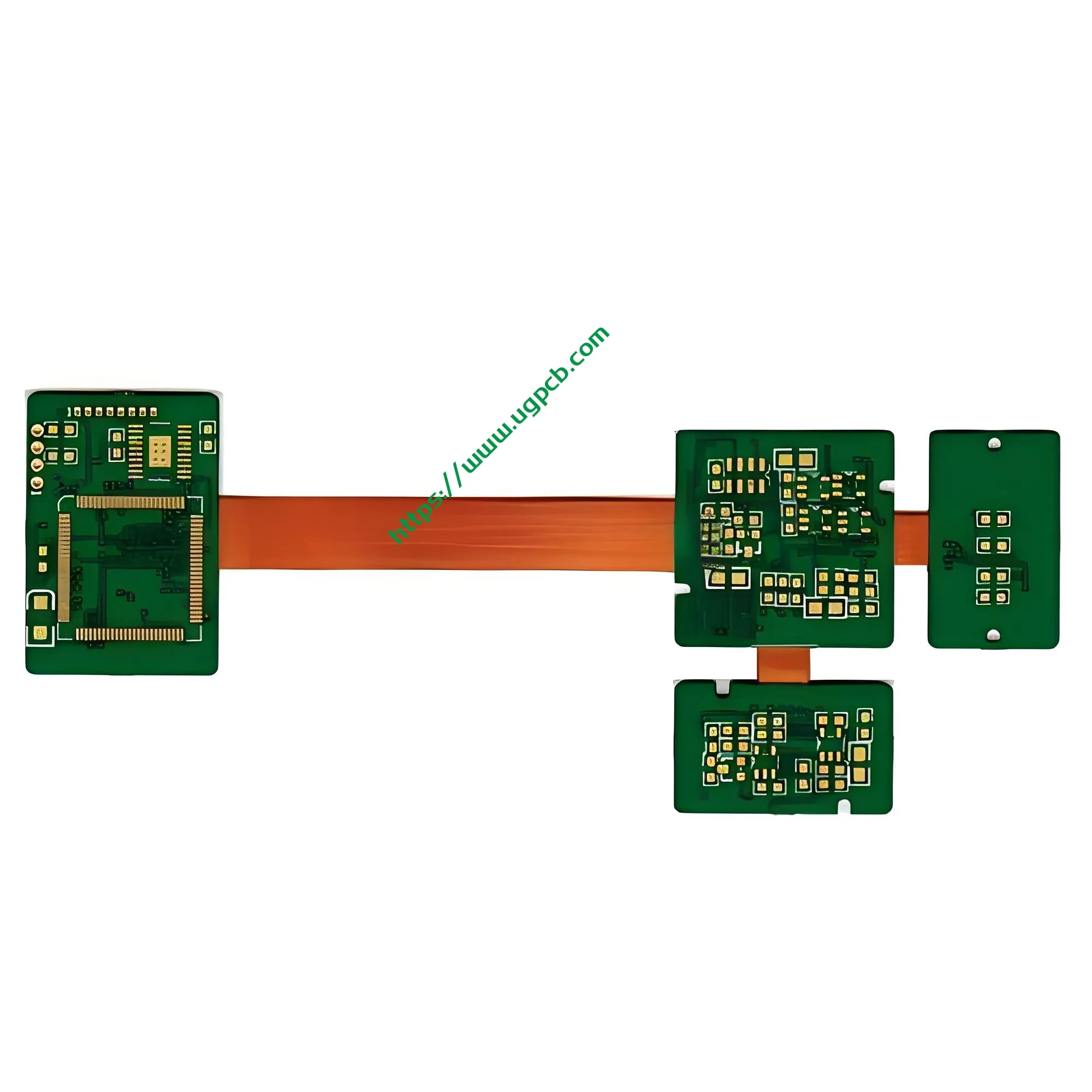
As electronic products move toward alta frequência, de alta velocidade, leve, and foldable projetos, traditional rigid PCBs or flexible printed circuits (FPCs) alone can no longer meet the demands of complex RF modules, smartphone cameras, or medical endoscopes. As a trusted leader in Fabricação de placas de circuito impresso, UGPCB apresenta o 8-Layer High Speed Rigid-Flex PCB. With its unique 6-camada rígida + 2-layer flex integrated structure, this board delivers an optimal balance of integridade do sinal, mechanical stability, e utilização do espaço.
This article provides a detailed overview of this PCB rígido-flexível—covering its definition, Materiais, processo de fabricação, and applications—to help you understand why it is the preferred choice for high-performance module PCBs.
1. Visão geral e definição do produto
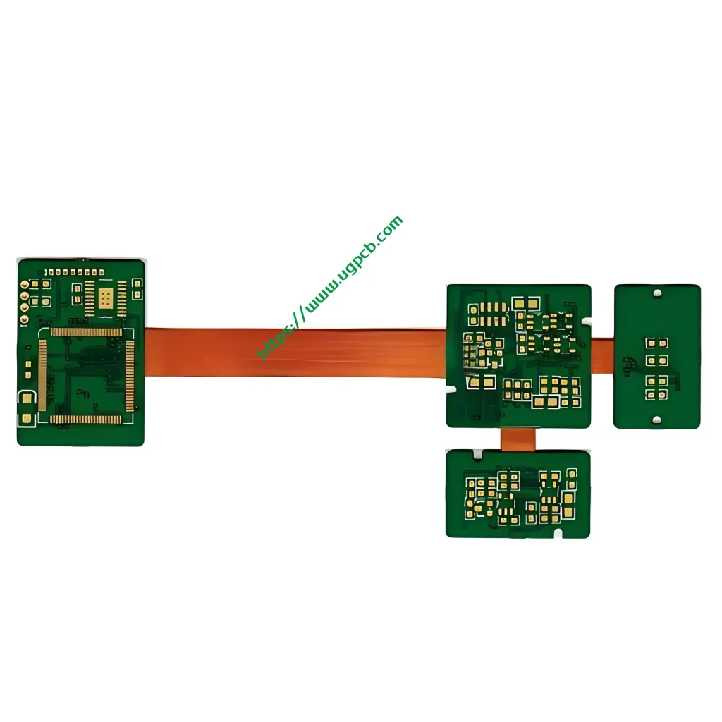
O8-Layer High Speed Rigid-Flex PCB is not simply a rigid board connected to a flex board via a connector. Em vez de, it is a unified structure formed by laminatingFR4 (rigid substrate) ePI (poliimida, flexible substrate) into a single component.
- Structure Breakdown: Rígido 6L (6-layer rigid section) + Flexível 2L (2-layer flexible section).
- Core Positioning: Ideal for compact electronic devices requiring high-speed signal transmission, dynamic flexing, e alta confiabilidade.
This design eliminates traditional board-to-board connectors, reducing solder joint failure risks while significantly improving compatibilidade eletromagnética (Emc) . It represents a key advancement in PCB de alta velocidade tecnologia.
2. Considerações de design e princípio de funcionamento
Considerações de design
When designing thisPCB rígido-flexível, UGPCB’s engineering team focuses on three critical areas:
- Controle de impedância: For high-speed signals, we strictly control trace width and spacing. This product achieves a minimum 3mil/3mil traço/espaço, ensuring consistent differential impedance (por exemplo, 90Ω or 100Ω).
- Proteção da Zona de Transição: The junction between rigid and flex sections is a stress concentration point. We apply teardrop compensation and optimized coverlay openings to prevent circuit breaks during dynamic bending.
- Simetria de empilhamento: To avoid warpage caused by CTE (coeficiente de expansão térmica) mismatch during high-temperature soldering, the rigid section uses a 6-layer symmetrical stack-up, while the flex section uses high-modulus PI material.
Princípio de funcionamento
O camada flexível (PI) acts as a bridge connecting multiple rigid functional modules. During bending, the flexible section transmits high-speed data signals (such as MIPI or USB 3.0) and power, while the rigid sections carry high-density BGA componentes and passive devices. This design enables the entire circuit system to fit into compact or irregular product enclosures.
3. Materials and Key Specifications
UGPCB uses premium materials from leading global brands to ensure electrical performance and reliability. Below are the key specifications for this model:
| Parâmetro | Especificação | Visão técnica |
|---|---|---|
| Material base | FR4 + PI | Rigid section uses high-Tg FR4 (Tg > 150°C) for soldering stability; flex section uses polyimide (PI) for flexibility and heat resistance. |
| Espessura do Cobre | 1 OZ | Finalizado 1 oz copper supports higher current loads and helps reduce skin effect loss insinais de alta velocidade. |
| Espessura da placa acabada | 1.0 milímetros | Balances mechanical support with thin device requirements. |
| Acabamento superficial | Imersão Ouro | 2eu” espessura do ouro. Fornece um apartamento, solderable surface with excellent oxidation resistance, ideal for fine-pitch BGAs and aluminum wire bonding. |
| Tamanho mínimo do orifício | 0.2 milímetros (mecânico) | Suportes interconexão de alta densidade (IDH) projetos; blind and buried vias can further save routing space. |
| Rastreamento Mínimo / Espaço | 3mil / 3mil | Fine-line capability for high-density routing, ensuring signal integrity at high frequencies. |
4. Product Classification and Structural Features
Classificação Científica
According to IPC-2223 standards, this product is classified as adynamic flex rigid-flex PCB.
- Por estrutura: Asymmetric rigid-flex (6-camada rígida + 2-layer flex).
- Por aplicação: De alta velocidade, alta frequência módulo PCB.
Características estruturais
- Integrated Interconnection: Eliminates connectors, reducing insertion loss and signal reflection. Signal integrity improves by approximately 30% compared to traditional rigid board plus connector solutions.
- High Flex Durability: The 2-layer flex section uses rolled annealed (RA) cobre, which offers better bending life than electrodeposited (DE) cobre, withstanding tens of thousands of dynamic bends.
- Thin and Light: With an overall thickness of 1.0 milímetros, it saves up to 60% of Z-axis space when folded.
5. Processo de Fabricação e Controle de Qualidade
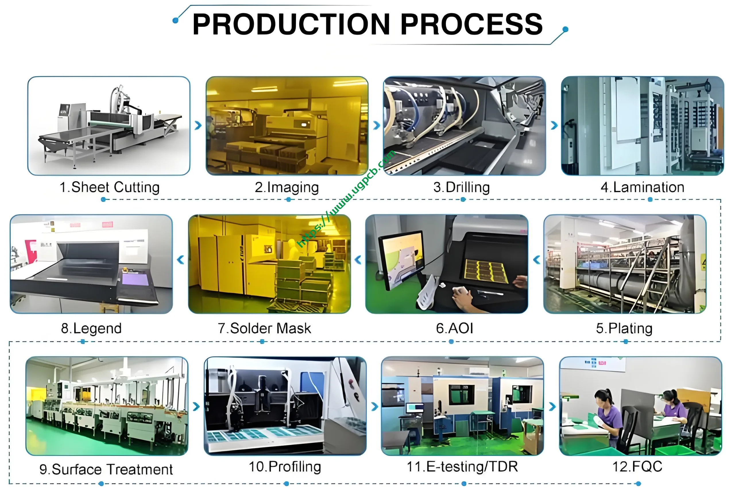
UGPCB operates a fully integrated production line to ensure everyhigh-speed rigid-flex PCB meets strict quality standards. The core process includes:
- Flex Layer Preparation: PI substrate is processed using inner-layer dry film and etching to form fine circuits (3mil trace width) in the flexible area.
- Laminação de capa: A coverlay is applied over the flex circuits to protect them and define the bending area.
- Rigid Layer Stacking: FR4 prepreg is precisely aligned with the processed flex layer. This is a critical step to ensure resin fills the rigid-flex interface without voids.
- Laminação: The rigid and flex layers are fused under high temperature and pressure.
- Perfuração e Chapeamento: 0.2 mm mechanical drilling is performed, followed by electroless copper plating to establish interlayer connections.
- Acabamento superficial: Ouro de imersão is applied with a controlled thickness of 2eu” to ensure solderability and oxidation resistance.
- Routing and Electrical Testing: Laser cutting or die punching shapes the board, seguido pela 100% flying probe or fixture testing to guarantee no shorts or opens.
6. Cenários de aplicação
Esse8-layer high-speed rigid-flex PCB is designed for high-density, high-reliability applications, incluindo:
- Smartphones and Wearables: Used in foldable phone mainboard connections and camera module (CCM) montagens, leveraging bending capabilities for hinge integration.
- Dispositivos médicos: Such as ultrasound endoscopes and hearing aids. The compact size and reliability of rigid-flex PCBs ensure stable signal transmission in critical environments.
- Eletrônica Automotiva: In-vehicle camera modules and LiDAR systems. Meets automotive-grade requirements for vibration resistance and temperature cycling (-40° C a 125 ° C.).
- Aeroespacial e Defesa: Satellite communication modules and missile guidance systems. Reduces weight while maintaining high reliability.
- Controle industrial: Robot joints and servo motor drives. The flex section absorbs mechanical stress from motion.
7. Por que escolher UGPCB?
Manufacturing rigid-flex PCBs presents technical challenges, particularly invoid-free lamination at the rigid-flex interface econtrolling material shrinkage of PI. UGPCB addresses these with proven expertise:
- Precise Shrinkage Compensation: With extensive data on the different expansion rates of PI and FR4, we maintain layer-to-layer registration within ±2 mil.
- High-Speed Signal Assurance: Para PCB de alta velocidade Aplicações, we strictly control dielectric constant (Dk) e fator de dissipação (Df), and provide impedance test reports.
- Customization Support: From prototypes to mass production, we support tailored módulo PCB solutions with reliable lead times.
8. Faça uma cotação hoje
Is your next-generation product still limited by connector size and signal loss? It’s time to upgrade to the8-Layer High Speed Rigid-Flex PCB.
[Entre em contato com os engenheiros do UGPCB] para:
Competitive Volume Pricing.
Free DFM Analysis Report (dentro de 24 horas).
Impedance Optimization Recommendations.