

Laboratorul este liniștit după miezul nopții. Diagrama ochilor de pe osciloscop pentru asta 28 Semnalul Gbps PAM4 pur și simplu refuză să se deschidă - jitter excesiv, margini zdrențuite — și ați verificat impedanța, potrivirea lungimii, și stivuire. Totul arată “standard.” Apoi măturați un TDR (reflectometru în domeniul timpului) de-a lungul urmei victimei și găsiți că forma de undă a zgomotului se potrivește cu marginea de comutare a liniei de ceas care merge chiar lângă ea. Aceasta nu este imaginație. Acesta este diafonia - transferul de energie silențios între două urme paralele.
Cuplaj capacitiv și cuplaj inductiv: Cele două căi ascunse
Diafonia apare din cuplarea electromagnetică între interconexiunile adiacente, mediat de două mecanisme distincte.
Cuplaj capacitiv transferă energie prin capacitatea parazită dintre urme. Cu cât schimbarea tensiunii este mai rapidă (dV/dt) pe linia agresorului, cu atât mai mult curent de zgomot injectează în linia victimă prin capacitatea reciprocăCₘ. Cuplaj inductiv transferă energie prin inductanță reciprocăLₘ — schimbarea actuală (di/dt) asupra agresorului induce o tensiune de zgomot asupra victimei.
Tensiunea totală de diafonie poate fi exprimată conform cadrului stabilit în IPC-2221, standardul de proiectare a fundației pentru plăci imprimate și alte structuri de montare sau interconectare a componentelor:
Vₙ = k × (V_d × C_d + I_d × L_d)
unde *k* este coeficientul de cuplare, CD este capacitatea distribuită, şiL_d este inductanța distribuită.
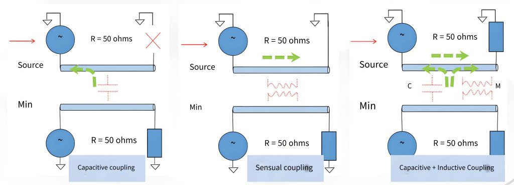
Datele măsurate prezintă o imagine clară. Pentru a 50 Ω microstrip line cu 8 mil urme lăţime şi 4 mil grosime dielectric, mărind distanţa de la 8 mil (1W) la 12 mil (1.5W) reduce vârful de diafonie capacitivă cu aproximativ 35%. Creșterea în continuare la 16 mil (2W) produce doar un suplimentar 9% reducere. Acest lucru indică faptul că dincolo de 3W (24 mil), beneficiul marginal scade brusc - amplitudinea diafoniei nu se scalează liniar cu spațierea, ci urmează o decădere exponențială.
Near End vs. Capătul îndepărtat: Direcții diferite, Comportamente diferite
Diafonie apropiată (URMĂTORUL) se cuplează înapoi către șofer la capătul de lansare al semnalului de agresor. Amplitudinea sa poate atinge 10% la 20% a semnalului de agresor, dar esteindependent de lungimea cuplajului — odată ce lungimea de cuplare depășește lungimea de saturație (aproximativ egal cu timpul de creștere a semnalului înmulțit cu jumătate din viteza de propagare), amplitudinea NEXT încetează să crească. NEXT depinde doar de geometria locală.
Diafonie la capătul îndepărtat (FEXT) apare la capătul îndepărtat al semnalului și amplitudinea acestuia este proporțională cu lungimea de cuplare - dar pierderea dielectrică suprimă componentele de înaltă frecvență, deci urme mai lungi produc uneoriMai puțin FEXT.
O 28 Simularea legăturii Gbps PAM4 ilustrează clar acest lucru: la 15 mm lungime cuplaj, maximul FEXT atinge -28 DB. Extinderea la 30 mm îmbunătățește FEXT la -31 dB datorită atenuării de înaltă frecvență.
Pe un plan de referință solid, contribuțiile capacitive și inductive la diafonie sunt aproximativ egale ca mărime. Pentru FEXT, sunt opuse ca polaritate și tind să se anuleze – motiv pentru careStructurile stripline prezintă intrinsec mai scăzută FEXT. Liniile microbande, cu toate acestea, au câmpuri electrice care trec parțial prin aer, creând un dezechilibru între cuplarea capacitivă și inductivă care face ca FEXT să nu fie neglijabil.
Regula 3W: Eficient, dar cu Precondiții
The “3regula W” este practic instinctiv pentru majoritatea PCB ingineri — menține distanța dintre urme de cel puțin trei ori lățimea urmelor. Dar mulți trec cu vederea condițiile sale prealabile.
Când distanța de la centru la centru ajunge la 3W, aproximativ 70% a energiei câmpului electric devine limitată în fiecare regiune dielectrică, reducerea capacității de cuplare la un nivel acceptabil. Diferite niveluri de spațiere produc următoarele caracteristici de atenuare a diafoniei:
| Spațierea urmelor | Atenuarea diafoniei | Evaluare |
|---|---|---|
| 1W | Aproximativ -20 DB | Semnificativ, inacceptabil |
| 2W | Aproximativ -30 DB | Moderat |
| 3W | Aproximativ -38 DB | Acceptabil pentru majoritatea modelelor |
| 4W | Aproximativ -42 DB | Excelent |
Regula 3W poate menține diafonia mai jos -35 DB, care este acceptabil pentru majoritatea modelelor. Cu toate acestea, această concluzie se bazează pe trei condiții prealabile: un plan de referință continuu, proprietăți dielectrice uniforme, și frecvențele de operare de mai jos 5 GHz.
Date măsurate pe a 50 Linia microbandă Ω arată că reducerea distanței de la 3W la 2W se degradează NEXT cu aproximativ 9 DB. Dacă planul de referință are goluri, degradarea sare la 15 DB. Pentru modelele de mai sus 28 GBPS (Frecvența Nyquist la 14 GHz), luați în considerare distanța de la 5W la 7W combinată cu tehnici suplimentare de suprimare.
Urme de gardă și control al căii de întoarcere: Mai eficient decât spațierea singură
Plasarea urmelor de gardă împământate de ambele părți ale liniei victimei, cu vias la sol fiecare 100 la 200 mil, poate reduce NEXT cu mai mult de 20 DB.
O 10 Studiul de caz Gbps backplane demonstrează eficacitatea: perechile LVDS adiacente fără împământare prin izolație sunt expuse 180 diafonie inductivă mVpp. Adăugarea unui rând de 0.3 mm împământare prin fiecare 10 mm a redus diafonia la 75 mVpp — o reducere de aproape 60%.
Figura 2: Urmărirea gardului cu Ground Via Array — Comparație pentru suprimarea diafoniei
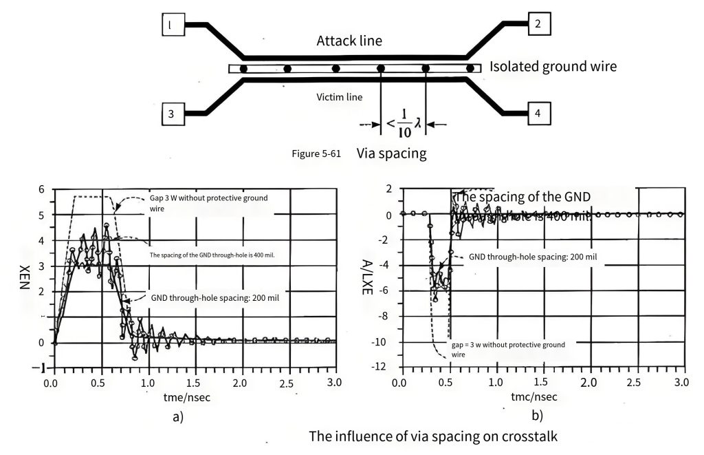
Considerente de proiectare a urmelor de gardă cheie:
- Mențineți o distanță de cel puțin 3 W între traseul de gardă și urmele semnalului pentru a evita cuplarea capacitivă suplimentară
- Păstrați prin spațiere la ≤ λ/10 (unde λ este lungimea de undă la cea mai mare frecvență a semnalului)
- Pentru 10 Semnale Gbps, limitați pământul prin spațierea matricei la cel mult 6 mm
Controlul căii de întoarcere se dovedește mai eficient decât simpla creștere a distanței. Reducerea distanței dintre semnal și planul de referință de la 8 mil to 4 mil sporește limitarea câmpului electric și reduce coeficientul de cuplare inductivă cu aproximativ 40%. Acesta este motivul pentru carerutarea semnalelor aproape de un plan de masă solid suprimă în mod inerent diafonia.
Diagnostic și strategie: Identificați mai întâi mecanismul dominant
Primul pas în suprimarea diafoniei nu este creșterea orbește spațierea sau adăugarea de urme de gardă, ci estediagnostic. Utilizați un TDR sau VNA pentru a mătura urmele victimei și a examina relația dintre forma de undă a zgomotului cuplat și semnalul agresorului:
- Zgomotîn fază cu agresorul →cuplaj capacitiv dominant → acordați prioritate măririi distanței, schimbarea straturilor, și scurtarea curselor paralele
- Zgomotdefazat cu agresorul →cuplaj inductiv dominant → acordați prioritate reducerii căii de întoarcere, rutarea mai aproape de planul solului, și adăugând urme de gardă
Managementul diafoniei se rezumă la a înțelege dacă domină cuplajul capacitiv sau inductiv, apoi aplicând remediul potrivit. Creșterea distanței adresează cuplarea capacitivă. Controlul căii de întoarcere se adresează cuplajului inductiv. Urmele și canalele de gardă oferă o plasă de siguranță completă. Nicio tehnică nu funcționează pentru fiecare scenariu.
Declarația surselor de date:
Referințele la standardele IPC din acest articol se bazează pe IPC-2221Standard generic pentru designul plăcii imprimate. Datele de atenuare a diafoniei regulii 3W fac referire la liniile directoare de proiectare standard din industrie și validarea simulării. The 28 Datele de simulare a legăturii Gbps PAM4 fac referire la literatura de proiectare a integrității semnalului de mare viteză. Descrierile mecanismelor de cuplare NEXT și FEXT fac referire la sursele manuale privind integritatea semnalului.
