
I. Market Catalyst: NVIDIA’s M10 Test Launches PCBs into the Ultra-High-Speed Era
In March 2026, a supply chain move by AI leader NVIDIA sent ripples through the electronics industry. Their next-generation Rubin platform officially initiated supplier testing for M10, a new Copper Clad Laminate (Ccl) material. This is more than a simple material upgrade. It signals the PCB industry’s official entry into a high-frequency, high-speed era. This new age is driven by AI and defined by ultra-low loss and exceptional signal integrity.
The M10 testing targets critical components for the Rubin Ultra and Feynman platforms. These include orthogonal backplanes and switch blade motherboards. Compared to the previous M9 generation, M10 introduces multiple suppliers. This breaks single-source dependencies. More importantly, it sets a new performance benchmark. Signal loss is projected to drop by 30-40% compared to traditional FR-4 PCBs. This is crucial for meeting the rigorous transmission speeds and thermal management demands of 800G/1.6T optical modules and high-performance computing. If testing proceeds smoothly, mass production is slated for the second half of 2027. This will trigger a new cycle of large-scale procurement for AI server PCB materials.

Ii. PCB: More Than Just a “Skeleton,” It’s the “Neural Center” of AI Computing
To understand this shift, we must first look at the PCB itself. PCB stands for Placă de circuit tipărită. It is often called the “Mother of Electronic Products.” It is a carrier where conductive circuits and connection holes are etched onto an insulating substrate, like a copper clad laminate.
Its core functions go far beyond physical support:
-
Electrical Connection: It provides stable circuit connections for all components. These include CPUs, GPUs, memorie, resistors, and capacitors.
-
Signal Transmission and Power Distribution: It ensures high-speed signals transmit without distortion. It also distributes power precisely to every component.
-
Heat Dissipation and Shielding: Under high-power AI chips, the PCB acts as an efficient heat path. It also provides electromagnetic shielding to ensure system stability.
Without high-performance PCBs, smartphones would not be so thin. Automotive electronics would not be as smart. The immense computing power of AI servers would be impossible. As AI computing demands surge, PCB technology is evolving. It is moving from traditional multilayer boards to advanced designs. These include higher layer counts, Interconectare de înaltă densitate (HDI), and rigid-flex structures.
Iii. 2026 PCB Industry Status and Competitive Landscape: O “Two-Tier” World Dominated by Chinese Manufacturing
De 2026, the PCB industry chain clearly shows “AI-driven” characteristics. The global competitive landscape is now sharply divided. On one side is China, dominating manufacturing scale. On the other are Japan, Taiwan, and South Korea, leading in high-end materials.
1. Deeply Optimized Demand Structure
The explosive growth of AI servers has directly reshaped PCB demand. Data shows that AI servers’ share of PCB demand jumped from 15% in 2025 to over 25% in 2026. The PCB value per AI server unit has increased by more than 30%. Layer counts have leaped from 16-20 layers to 28-36 straturi. This places extreme demands on manufacturing processes and materials.
2. Accelerating PCB Material Upgrades
NVIDIA’s M10 test marks a complete industry shift from standard FR-4. The move is toward ultra-low loss materials like M8, M10, and Panasonic’s Megtron series. Leading domestic CCL manufacturers have also started small-batch validation. This meets the needs of AI servers and 400G/800G high-speed optical modules.
3. The Global “Two-Tier” Competitive Landscape
-
Tier 1 (Manufacturing Dominance): Mainland China. As the world’s largest PCB production base, China’s capacity share remains stable at over 55%. Leveraging massive scale, fastest turnaround, and lowest cost, Chinese manufacturers have developed world-class capabilities in multilayer and Panouri HDI.
-
Tier 2 (Material Leadership): Japonia, Taiwan, Coreea de Sud.
-
Japonia: Holds the highest technological barriers in high-end materials. Companies like Panasonic and Sumitomo dominate the low-loss CCL market.
-
Taiwan: Companies like Taiwan Union Technology Corporation (TUC) and Iteq have a strong market share in high-frequency, high-speed CCLs. They hold about 18% of the global market.
-
Coreea de Sud: Samsung Electro-Mechanics is a strong player in automotive PCBs and high-end HDI.
-
The industry chain division of labor is exceptionally clear. High-end materials upstream are controlled by Japan, Taiwan, and South Korea. These include specialty resins, ultra-thin glass fiber, and HVLP copper foil. Midstream Fabricarea PCB-urilor is dominated by Mainland China. În aval, global AI, auto, and communication brands drive final applications.
Iv. Growth Forecast: A Defined Growth Path in the AI Era
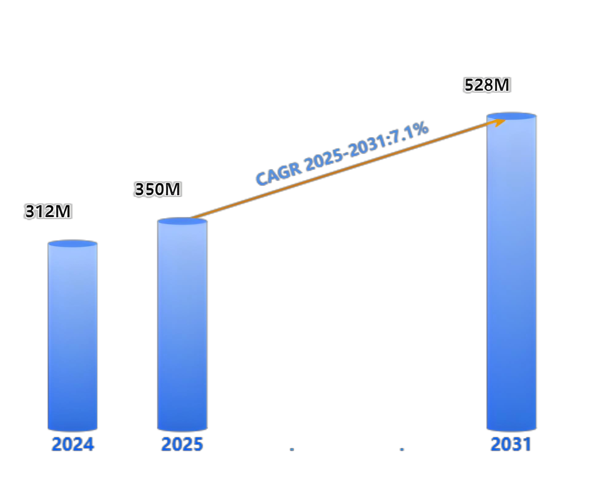
PCB is a primary and direct beneficiary of the AI computing boom. It offers high growth certainty. According to IEK data, global PCB output was estimated at approximately 92.36 billion U.S. dollars in 2025. This represents an annual growth rate of 15.4%. Looking ahead to 2026, as AI infrastructure expands, the global PCB market is projected to reach 105.2 billion U.S. dollars. This is a growth rate of 13.9%. Some forecasts predict the global PCB market could exceed 137.8 billion U.S. dollars by 2035.
We can break down this growth into three phases:
-
Short-Term (2026-2027): The AI Server Volume Driver Phase. A compound annual growth rate (CAGR) de 28% la 35%. With the mass production of new materials like NVIDIA’s M10, high-end PCB orders will surge.
-
Mid-Term (2028-2030): The Multi-Driver Phase. This includes automotive electronics and 5G or 6G technologies. The expected CAGR is 22% la 28%. Automotive PCB creştere, driven by ADAS and domain controllers, could hit 40% annually.
-
Long-Term (2030 and beyond): The Full-Scenario Penetration Phase. A CAGR remaining above 18%. Mainland China’s share of the global PCB market is expected to stabilize between 58% şi 62%.
V. Core Industry Chain Analysis: Din “Three Main Materials” to High-End Manufacturing
The AI-driven PCB upgrade starts with stricter demands on upstream core materials. According to Huajin Securities, the high-end copper foil, electronic cloth, and specialty resins needed for advanced CCLs are undergoing capacity expansion and upgrades.
1. Upstream Materials: The “Genes” Determining Performance
-
Folie de cupru: Trends towards ultra-thin and low profile. HVLP copper foil is becoming the top choice for AI server CCLs. HVLP stands for High Very Low Profile. Its low loss characteristic is vital for high-speed transmission. The high-end market is currently dominated by foreign firms like Mitsui Kinzoku. Cu toate acestea, domestic companies such as Tongguan Copper Foil and Defu Technology are rapidly entering the supply chain.
-
Electronic Resin: This is the most designable part of the CCL formula. It determines the board’s dielectric properties, namely Dk and Df. To lower dielectric loss, materials are upgrading from traditional epoxy. New systems include PPO, EIP, BMI, hydrocarbon resins, and even PTFE. Domestic firms like Shengquan Group and Dongcai Technology have achieved mass production and supply of these resins.
-
Glass Fiber Cloth: Moving towards ultra-thin and low-dielectric types. To meet M10 grade processing requirements, next-generation materials may use quartz fiber. This would replace traditional electronic grade glass cloth. This further enhances signal integrity and stability.
2. Midstream Manufacturing: The Ultimate Test of Process Precision
High-end PCB manufacturing involves many critical steps. These include inner layer imaging, lamination, foraj, placare, and soldermask application.
-
Foraj: Hole diameters for AI server PCBs are now at the micron level. HDI boards require laser drilling instead of traditional mechanical drilling. This meets high precision needs. Domestic equipment makers like Han’s CNC now lead in this area.
-
Placare: For better hole uniformity and environmental friendliness, Vertical Continuous Plating (VCP) technology is now the mainstream choice for new production lines.
-
Key Metrics: Take high-layer boards with 18 or more layers as an example. Their share is expected to jump from 2.48% in 2024 la 5.3% de 2029. This represents a CAGR of 15.7% .
VI. How to Choose a Reliable PCB Supplier?
As the AI wave surges, choosing a technically capable and reliable PCB supplier is crucial. This applies whether you need prototyping or mass production. Facing numerous options, consider these points:
-
Material Certification Ability: Does the supplier have small-batch validation capabilities for high-frequency materials? De exemplu, M7 or M8 grades. Can they recommend the best Copper Clad Laminate (Ccl) for your specific design?
-
Process Capability: Can they handle over 30 straturi? Can they achieve minimum line widths and spacing below 25 micrometers, or even 20 micrometers? Can they support 4th order HDI or higher?
-
Controlul calității: Are they certified to international standards? Key certifications include IPC-A-600 for the acceptability of printed boards. Asemenea, IPC-6012 covers the qualification and performance specification for rigid printed boards. Do they have strict procedures for controlul impedanței and reliability testing?
If you are looking for an advanced Producător de PCB ready for AI-era challenges, get a quote online. You can also buy PCB online by submitting your requirements directly. Leading manufacturers like Shennan Circuits, WUS Printed Circuit, and UGPCB are expanding their high-end HDI and high-layer production. They are providing competitive solutions to customers worldwide.
Concluzie
From NVIDIA’s M10 material tests to the global PCB market reaching towards one hundred billion dollars, a golden age for high-end manufacturing has begun. The PCB is no longer just the “skeleton” of electronic products. It has become the “neural center” determining success in AI computing. For industry professionals, understanding this shift is key. It is a move from “scale expansion” la “value reconstruction.” This understanding will be vital for capturing the pulse of the electronics industry for the next decade.
