Нарушая ограничения: Передовые возможности UGPCB по проектированию подложек для микросхем
В эпоху взрывного роста вычислительной мощности искусственного интеллекта и расширения пропускной способности 5G/6G, Чипы размером с ноготь теперь включают в себя миллиарды транзисторов. Еще 60% отказов высокопроизводительных чипов происходят не от самих кремниевых пластин, но от дефектов их критического носителя – Подложка ИС. Эта поразительная статистика подчеркивает чрезвычайную важность дизайна подложки..
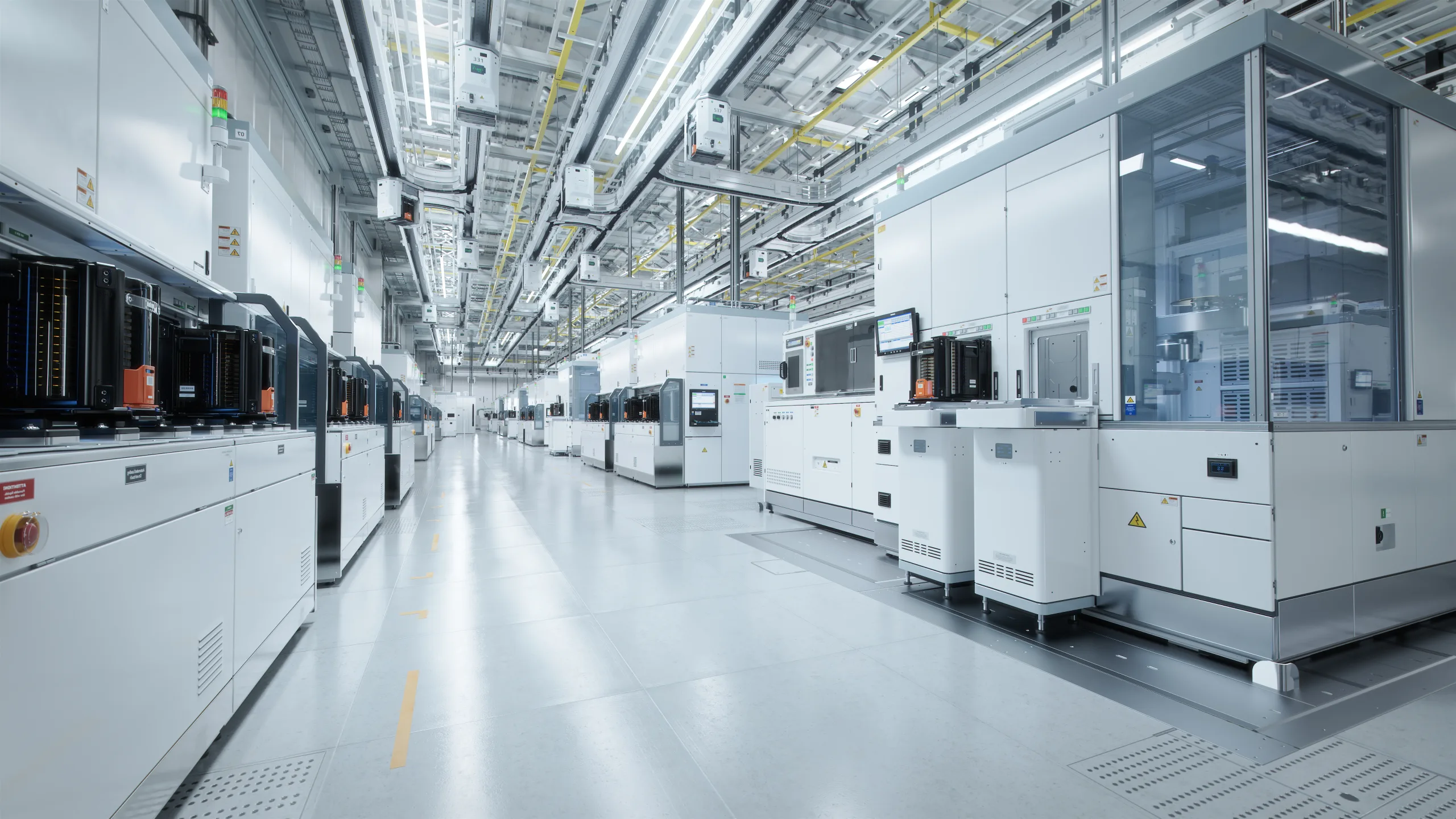
IC субстраты: Невидимый фундамент производительности чипов
Подложки микросхем — это гораздо больше, чем просто разъемы.; они служат нейронным центром и силовым ядром между чипами и внешним миром.. Число операций ввода-вывода возрастает до тысяч (даже 10,000+ для продвинутых графических процессоров/процессоров), ширина дорожек/расстояние уменьшаются ниже 15 мкм/15 мкм, и скорости сигнала, превышающие 112 Гбит/с., точность проектирования теперь работает в нанометровом масштабе. Сбои управления температурным режимом и ухудшение целостности сигнала стали лидерами в сфере современной упаковки (2.5Д/3D ИС, Чиплет).
Ключевая формула: Точность контроля импеданса (З)
Z = (87 / √εr) × ln(5.98H / (0.8W + T))
Где εr = диэлектрическая проницаемость, H = толщина диэлектрика, W = ширина дорожки, T = толщина меди. UGPCB точно контролирует эти параметры для достижения допуска по сопротивлению ±5%, что превосходит отраслевой стандарт ±10%..
Деконструкция UGPCB 5 Возможности проектирования основных подложек микросхем
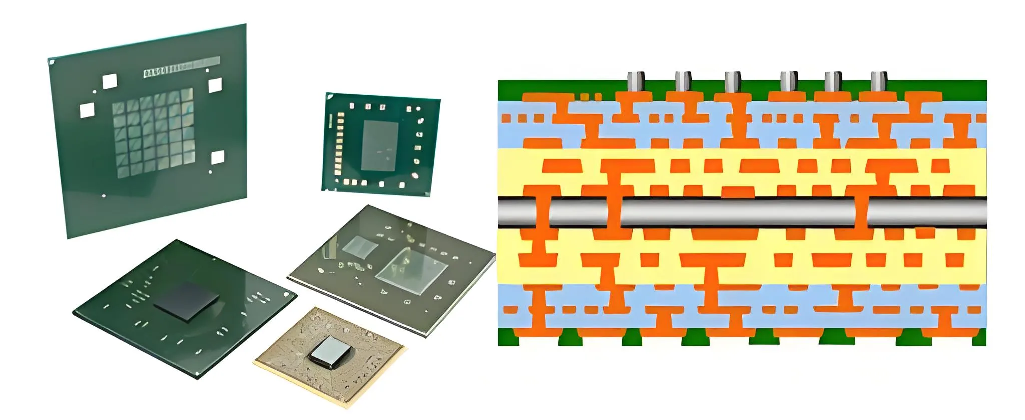
1. Межсоединение чрезвычайно высокой плотности (ИЧР) Дизайн
-
Мастерство микровии: Лазерное бурение (<50мкм) и расширенное покрытие позволяют ИЧР любого уровня. Улучшает каналы маршрутизации за счет 40% в исполнении BGA с шагом 0,2 мм.
-
Прорыв в сверхтонких линиях: Массовое производство дорожек толщиной 12 мкм/12 мкм отвечает передовым требованиям чиплетов..
-
Расширенные стеки: Экспертиза в 16+ многослойные конструкции с использованием гибридных материалов (низкий Dk/Df + высокий ТГ) для гетерогенной интеграции.
2. Наномасштабная целостность сигнала/питания (СИ/ПИ) Контроль
-
3D ЭМ моделирование: Ansys HFSS и Cadence Sigrity устраняют отражения и перекрестные помехи в каналах 112G PAM4.
-
Оптимизация ПДН: Распределенные сети развязки снижают шум источника питания (ПСН) к 60%.
-
Контроль потерь: Ультранизкопрофильная медь (RTF/VLP) в сочетании с соблюдением формулы импеданса минимизирует вносимые потери.
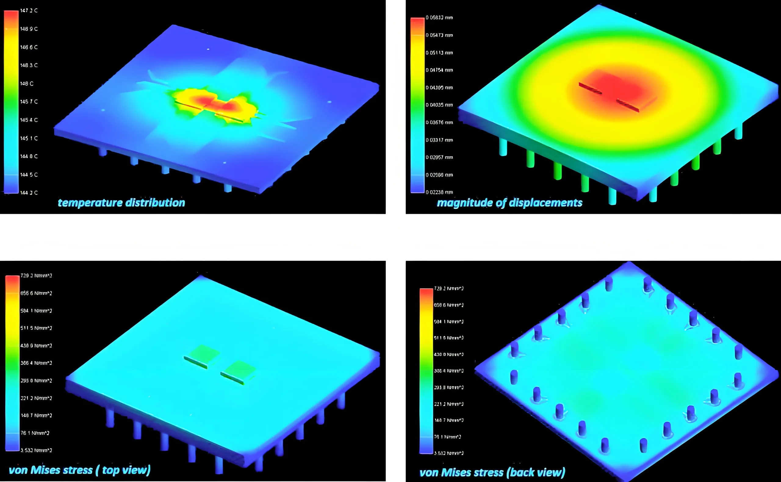
3. Тепломеханическая надежность (ТМВ) Инженерное дело
-
Соответствие CTE: Инновационный материалы минимизировать коробление (<0.1%) путем балансировки чипа (~2,6 частей на миллион/°C) и КТР подложки (14-17 ppm/° C.).
-
Мультифизическое моделирование: COMSOL прогнозирует усталость паяных соединений во время термоциклирования.
-
Тепловая Архитектура: Встроенные тепловые трубки + >5 Вт/мК TIM + оптимизированное охлаждение системы наддува тепловых переходов.
4. Усовершенствованная упаковка совместного дизайна
-
Сотрудничество Fab/OSAT: Ранняя интеграция DFM для FCBGA, WLP, и процессы промежуточного устройства Si.
-
Экспертиза чиплетов: Совместимость с UCIe и высокой пропускной способностью, межсоединения с низкой задержкой.
-
Материальная наука: Стратегическое использование Ajinomoto ABF, Серия MEGTRON для нужд RF/термографии/надежности.
5. Проектирование на основе DFM/DFT
-
Технологичность: Правила проектирования, соответствующие возможностям процесса, максимизируют выход с первого прохода (ФПЮ).
-
Оптимизация тестируемости: Удобная для ATE схема расположения контрольных точек для сложных материалов.
-
Дизайн для повышения доходности (ДФЮ): Балансировка меди и компенсация травления повышают стабильность производства.
История успеха УГКПБ: От дизайна до массового производства
Случай: Подложка мощного ускорителя искусственного интеллекта FCBGA
-
Испытание: 45×матрица 45 мм, >800Мощность Вт, 56Сигналы PAM4 Гбит/с, требующие экстремальных тепловых и электрических характеристик.
-
Решение:
-
16-слой любой-слой ИЧР со следами 12 мкм/12 мкм
-
ТРОН МЕНЯ 7 основной (εр=3,3, Дф=0,001) + прецизионный контроль импеданса
-
Встроенные медные блоки + массивы микропереходов (35% снижение термического сопротивления)
-
Совместное проектирование с OSAT для оптимизации неровностей и маршрутов.
-
-
Результат: Пройдена SI/PI/термическая проверка с первого раза, 98.5% урожай, 6-на месяц быстрее время выхода на рынок.
Почему мировые лидеры выбирают UGPCB в качестве партнера по подложкам для ИС
С 100+ опытные инженеры, 300+ ежегодные проекты подложек ИС, 20+ патенты, и лаборатории моделирования стоимостью в несколько миллионов долларов, УГКПБ доставляет:
Ключевые отличия
-
Технологическое лидерство: Определение границ подложки нового поколения с помощью R&Дюймовый.
-
Комплексные решения: Проектирование → Прототип → Серийное производство под одной крышей.
-
Уверенность в производстве: Собственные передовые фабрики обеспечивают реализацию дизайнерского замысла.
-
24/7 Отзывчивость: Выделенные группы поддержки с мгновенными котировками.
Раскройте весь потенциал вашего чипа сегодня!
Ограничен ли ваш флагманский чип следующего поколения узкими местами подложки?? Специалисты УГКПБ готовы предоставить:
✅ Бесплатная оценка осуществимости конструкции подложки ИС
✅ Расценки на конкурентные решения для печатных плат в 24 Часы
[Свяжитесь с экспертами UGPCB по IC-подложкам прямо сейчас для получения мгновенной поддержки & Цитировать]
Вичат
Сканируйте QR-код с помощью WeChat