УГКПБ: Leading IC Substrate Process Technology Delivering Reliable Solutions for High-End Chip Packaging
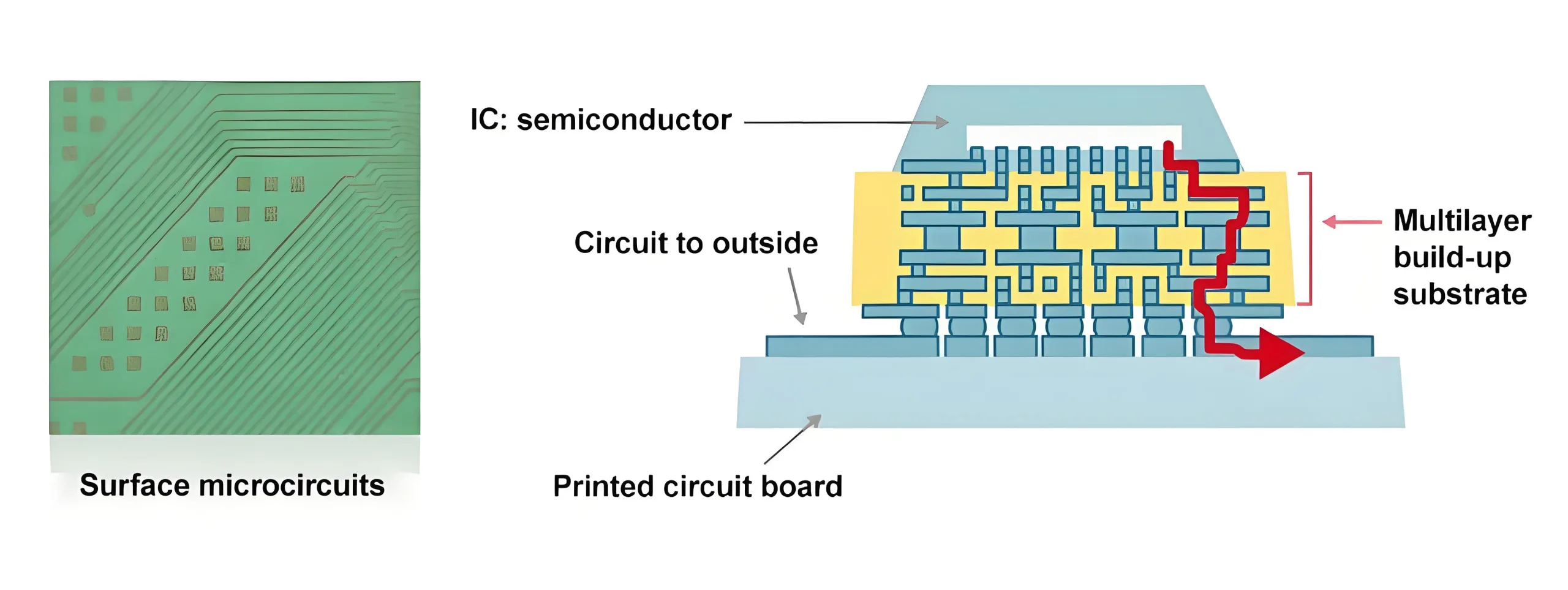
В сегодняшней быстро развивающейся электронике индустрии, Подложки ИС serve as the core foundation for chip packaging. They play a decisive role in the performance and reliability of cutting-edge applications including 5G, Ай, высокопроизводительные вычисления (HPC), и новые энергетические транспортные средства.
As essential materials in electronic packaging, nearly all chips across various electronic devices rely on substrates. Their quality directly influences the functionality and durability of advanced technologies such as 5G, 6Г, Ай, и высокопроизводительные вычисления.
With years of technical expertise and continuous innovation, УГКПБ has achieved groundbreaking progress in IC substrate manufacturing. We deliver high-precision and highly reliable IC substrates that meet the stringent demands of advanced semiconductor packaging.
IC Substrate Process Capability at UGPCB
UGPCB is committed to providing world-class IC substrate manufacturing services. Our process capabilities have reached internationally advanced levels:
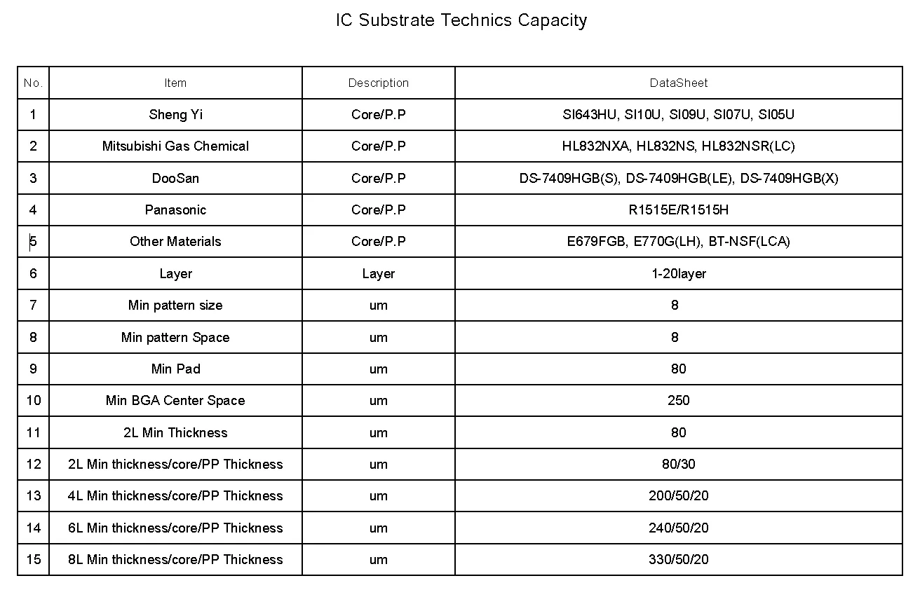
Layer Count and Dimensions: Our IC substrates support high-layer structures ranging from 2–10 layers to over 20 слои. Board thickness ranges from 0.08 мм до 11.2 мм, with maximum dimensions up to 105 × 105 мм, meeting the requirements of complex chip packaging.
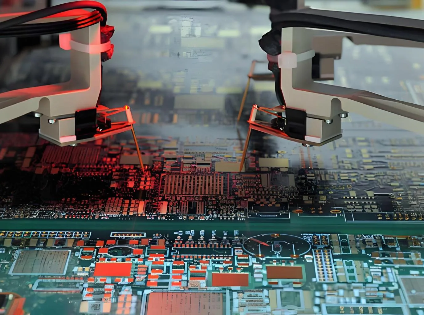
Fine Line Processing: Utilizing advanced modified Semi-Additive Process (Мсап) технология, UGPCB achieves exceptional fine-line patterning. Our trace width/spacing capability reaches an impressive 8μm/8μm—one-tenth the diameter of a human hair—significantly exceeding the standard 50μm/50μm level of conventional PCBs.
High-Precision Registration Technology: We employ automated alignment and parallel exposure technology to control layer-to-layer registration within ±5μm, greatly enhancing product yield and reliability.
Technical Advantages and Innovations at UGPCB
-
Advanced Lithography Process
УГКПБ использует Лазерная прямая визуализация (LDI) технология, eliminating dimensional variations associated with traditional contact printing and enabling tighter alignment tolerance. Our LDI system offers high and continuous Depth of Focus (DOF) and advanced compensation mechanisms, allowing high-precision imaging even on uneven surface topographies.
“Setting the correct DOF is crucial for achieving optimal resolution. Incorrect DOF settings may lead to trace width or spacing deviations, disconnections, or meandering defects.”
-
Precision Etching Control Technology
We maintain strict control over key parameters in the etching process. When using alkaline ammonia etching, the solution’s pH is kept between 8.0 и 8.2, effectively reducing undercut and side etching. Our etch factor formula is as follows:
Etch Factor (EF) = D / (U – Дюймовый) × 2
Where D is etch depth and U is undercut width. UGPCB maintains an etch factor above 3.0, ensuring vertical sidewalls and dimensional accuracy.
-
Rigid-Flex and Micro-Via Filling Technology
We have developed rigid-flex IC substrate technology that uses high-Tg non-flow prepreg and pure copper foil, enabling 4-layer rigid-flex substrates with total thickness ≤240μm and thickness tolerance within ±5μm.
Our micro-via filling plating technology overcomes critical technical challenges, increasing yield for 1–4 layer blind and buried vias by more than 30%.
Quality Control and Testing Capability at UGPCB
UGPCB has established a comprehensive quality control system supported by advanced inspection equipment:
-
Scanning Electron Microscope (Который): For analyzing fine circuit structures and defect causes
-
Fourier Transform Infrared Spectroscopy (FTIR): For material analysis and quality control
-
X-Ray Diffraction (XRD): For material crystal structure analysis
-
Thermal Cycle Shock Test Chamber: For product reliability testing
We implement strict warpage control standards. Warpage is calculated using the following formula:
Warpage = (час / л) × 100%
Where h is the maximum warpage height and L is the diagonal length. We control warpage below 0.5%, far exceeding standard PCB industry levels.
Applications and Service Advantages of UGPCB
UGPCB’s IC substrates are widely used in various high-end applications:
-
AI Chips and GPU/CPU Packaging: Our HDI and IC substrate equipment support AI chip manufacturing
-
5G/6G Communication Equipment: Low-loss substrate solutions for high-frequency applications
-
New Energy Vehicle Electronics: Automotive-grade IC substrates meeting high-reliability requirements
-
Memory Chip Packaging: Supports 20μm/20μm trace/space, with ongoing development toward 15μm/15μm
We provide one-stop PCBA services, covering the entire process from печатная плата manufacturing and Компонентная закупка to assembly and testing. Customers only need to provide PCB design files—we handle the rest, significantly reducing time and cost.
Заключение
With advanced technical equipment, strict quality control, and extensive experience, UGPCB has achieved remarkable accomplishments in IC substrate manufacturing, breaking foreign technology monopolies and filling domestic gaps.
We remain dedicated to technological innovation and quality improvement, providing global customers with superior and reliable IC substrates and печатная плата services to help them achieve greater success in high-end electronics.
Contact UGPCB today to experience the value our advanced IC substrate process technology can bring to your projects!
Вичат
Сканируйте QR-код с помощью WeChat