
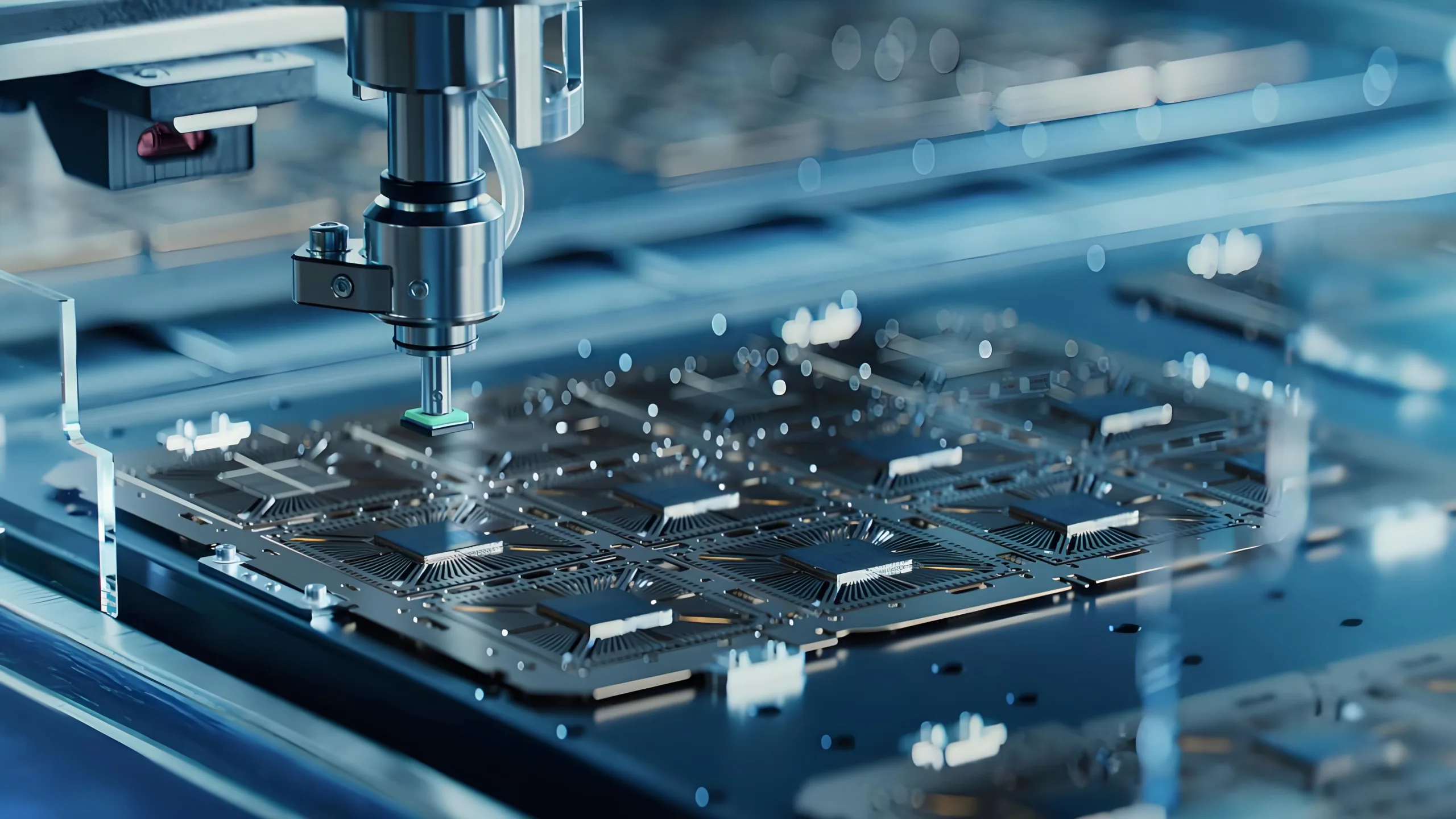
Полупроводниковые чипы служат “мозги” цифровой эры, В то время как упаковка Chip действует как их защитный “доспехи” и “Нейронная сеть.” За пределами экранирования хрупкого кремния умирает, это позволяет критическое тепловое управление, электрическая связь, и передача сигнала. От громоздких пакетов до сверхтонких решений на уровне пластины, Эволюция упаковки имеет миниатюризацию и повышение производительности электроники - монументальная технологическая сага.
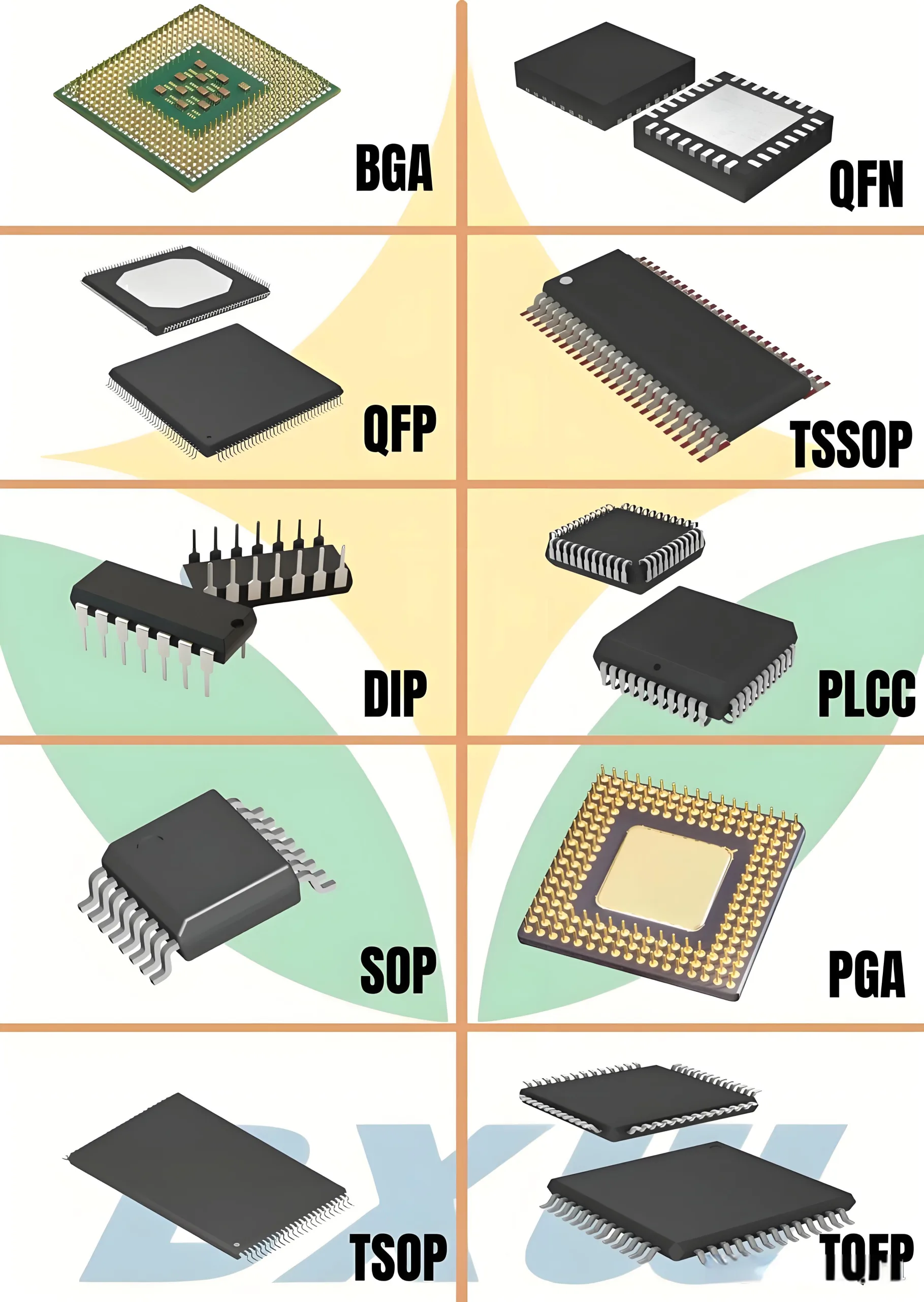
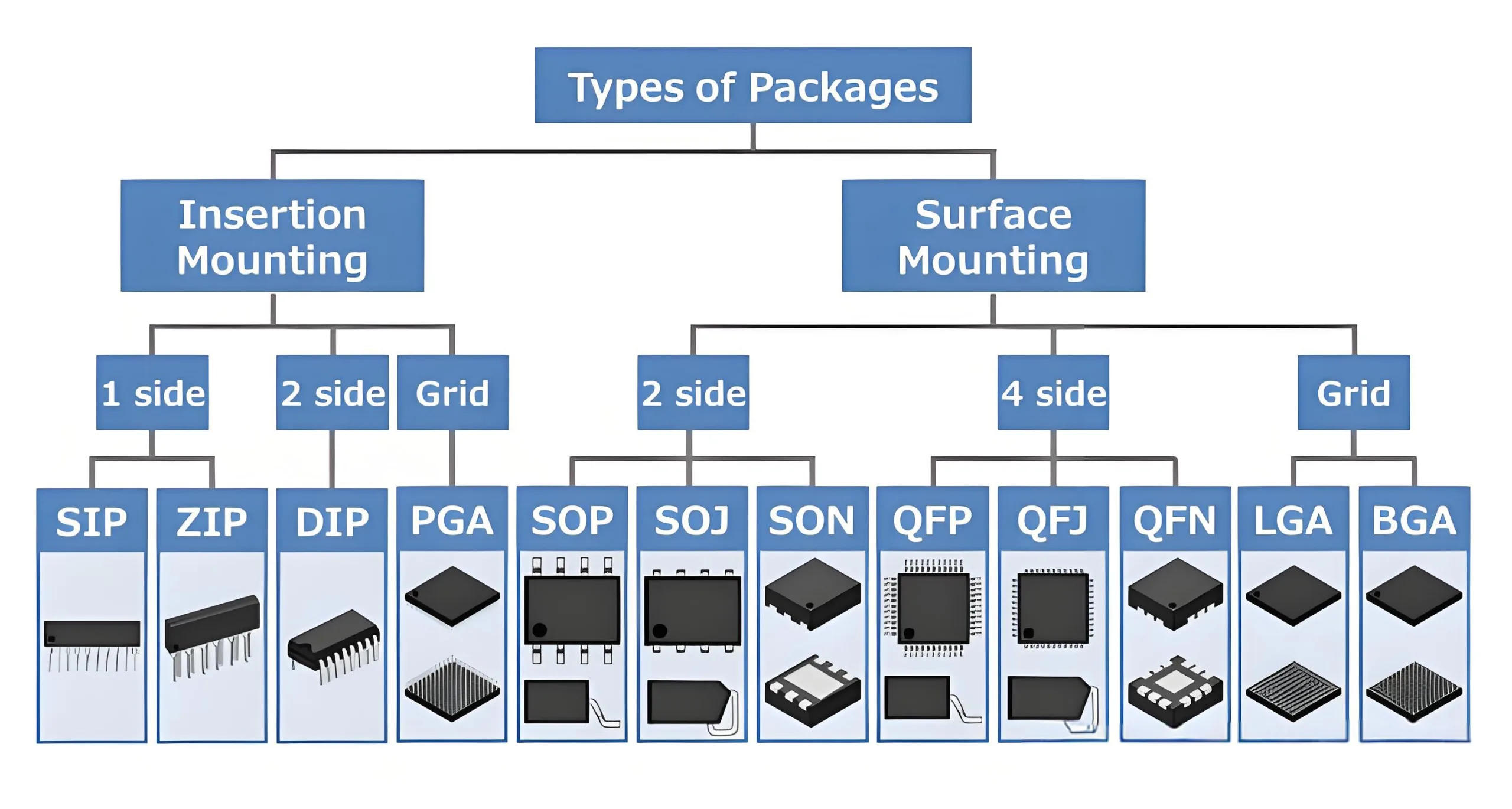
Классификация технологий упаковки
Методом монтажа
-
Упаковка сквозной дыры (ТТТ):
Булавки вставлены в печатная плата нанесит на вылову через пайку. Представляет технологию раннего поколения. -
Поверхностная технология (СМТ):
Компоненты непосредственно припаяны на прокладки платы. Обеспечивает более высокую плотность и автоматизированную сборку.
Конфигурацией PIN (Плотность прогрессии)
Одно рядовой → двойной → четырехсторонний →
Эпоха сквозного
До/до: Основы дискретных компонентов
-
Do-41 диод: Ø2,7 мм × 5,2 мм
-
К 220 транзистор: Ручки ≤50 Вт рассеяние мощности
-
Тепловое сопротивление: Р<подставка>и</подставка> = (Т<подставка>Дж</подставка> – Т<подставка>а</подставка>)/П
Где Р<подставка>и</подставка> = тепловое сопротивление соединения к ямке
SIP/Zip: Одно встроенные инновации
-
ГЛОТОК: 3-16 булавки, Эффективный для резисторов/диодов с низким энергопотреблением
-
Молния: 40% Более высокая плотность штифтов, чем SIP с помощью зигзагообразного устранения
-
Приложения: Модули ранней памяти, регуляторы напряжения
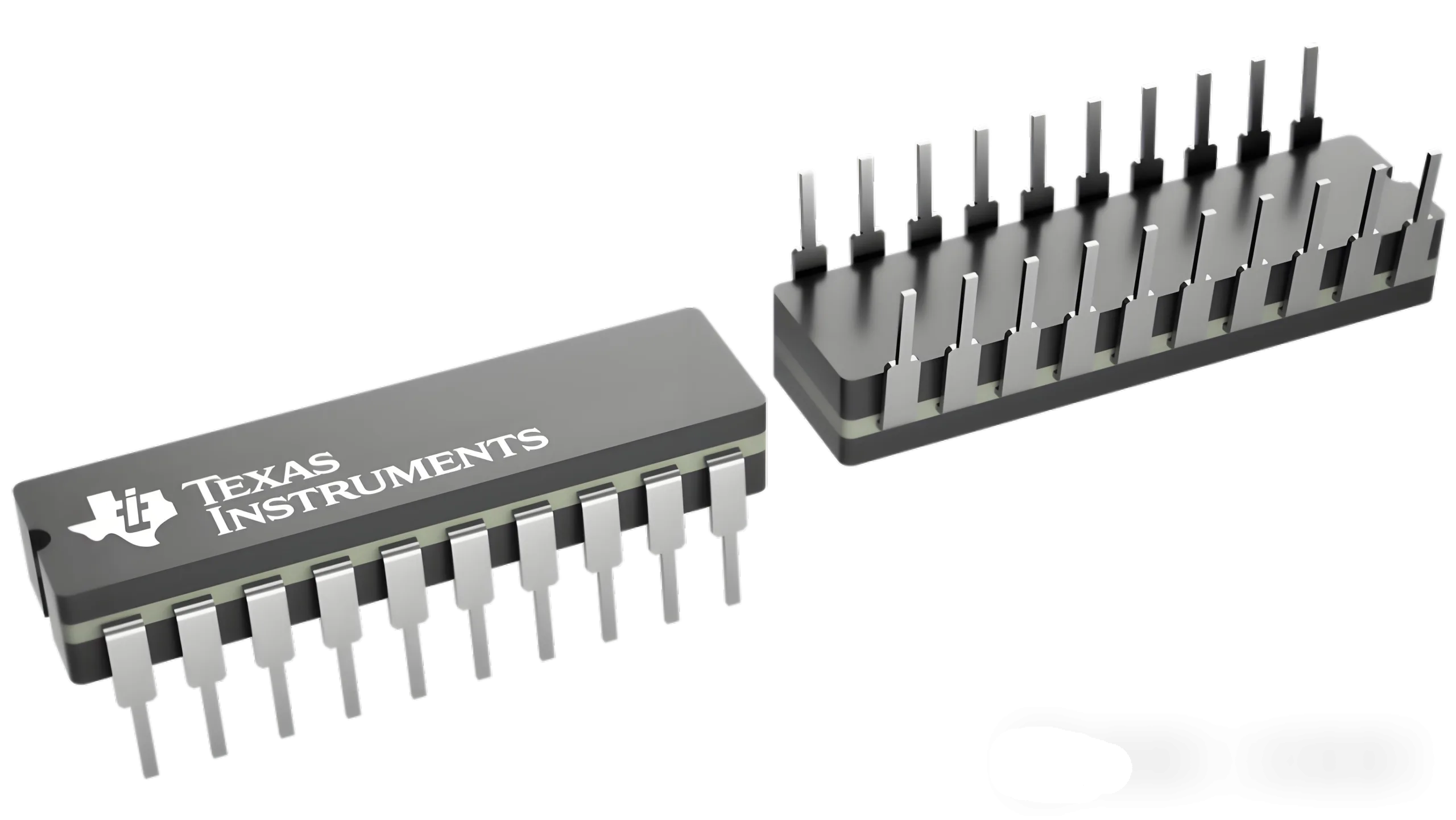
ОКУНАТЬ: Революция IC
-
Штифт: 2.54мм (0.1″) стандартный
-
1980S Рыночная доля: >70% IC упаковки
-
Тепловые характеристики:
Керамический соус: 20-30 W/m · k -проводимость
Пластиковый падение: 0.2-0.3 W/m · k
Пг: Высокопроизводительный пионер
-
Плотность штифтов: 3× выше, чем DIP
-
Приложения: Intel 80386/80486 процессоры
-
Вставка силы: 30-100 Ньютоны
SMT Революция
SOD/SOT: Дискретная компонента миниатюризации
-
SOD-323: 1.7мм × 1,25 мм
-
SOT-23 Термическое сопротивление: ~ 250 ° C/W.
-
Профиль режни: Пик температура 235-245 ° C.
Гулл-крылат: Семья СОП
-
Эволюция штифта:
1.27мм (Соп) → 0,8 мм (SSOP) → 0,65 мм (TSSOP) -
Производные пакеты:
SOP → SSOP → TSOP → TSSOP → VSSOP -
Тепловое улучшение: HSSOP снижает тепловое сопротивление 40%
J-Lead Configuration: Наблюдение
-
Механическая прочность: 30% Более высокая стресс -сопротивление
-
Электрическое ограничение: 0.8-1.2NH Паразитарная индуктивность
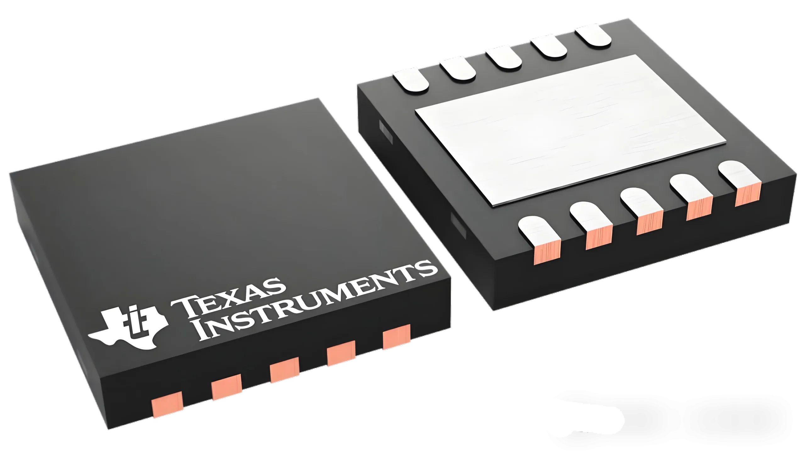
Прорыв без свинца: Сын/DFN
-
Космическая эффективность: >50% Улучшение по сравнению с SOP
-
Тепловые характеристики: 15° C/W с тепловыми прокладками
-
Миниатюризация предела:
X2son: 0.6мм × 0,6 мм × 0,32 мм
Физика, стоящая за миниатюризацией
Три основные проблемы регулируют масштабирование пакетов:
-
Тепловое управление:
Q = haΔt
Уменьшенный размер (↓ а) требует более высокого коэффициента конвекции (↑ ч) -
Управление тепловым напряжением:
S = eptt
Где Cte (а) Несоответствие вызывает стресс -
Целостность сигнала:
Индуктивность свинца *l ≈ 2L(ведущий(2L/D.)-1) nh*
Миниатюризация снижает индуктивность 30%
Следующая граница: Усовершенствованная упаковка
Поскольку x2son достигает 0,6 мм масштаба, Инновации переходят к:
-
3D Упаковка: Вертикальная интеграция с поддержкой TSV
-
Гетерогенная интеграция: Многолетняя умирающая сборка
-
Фотоника: Совместный кремниевый фотоникс
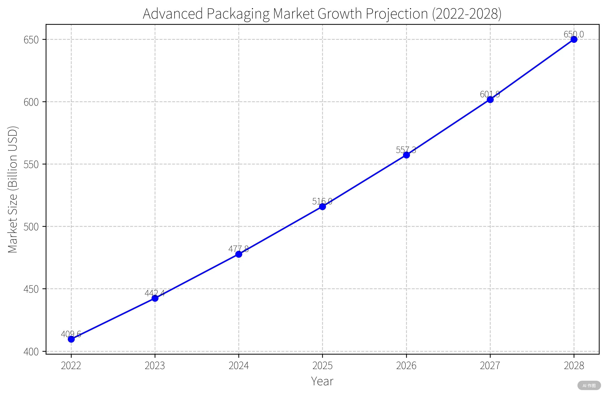
Прогноз рынка (Йоль девелоппендия):
8% CAGR через 2028 → Рынок 65 млрд долларов
Упаковка теперь критически определяет производительность системы - далеко за пределами простой защиты.
Заключение
От 2,54 мм шага до 0,6 мм X2SON., Достижения упаковки непрерывно переопределяют электронику. Каждый тонкий смартфон и 5G -устройства полагаются на эти невидимые инновации. С появлением ИИ и квантовых вычислений, Чип -упаковка будет продолжать раздвигать наноразмерные границы.
*Далее в серии:
BGA/CSP/WLCSP Technologies
3D Упаковка & TSV Interconnects
Усовершенствованная упаковка материаловая наука
Следите за обновлениями!*
