
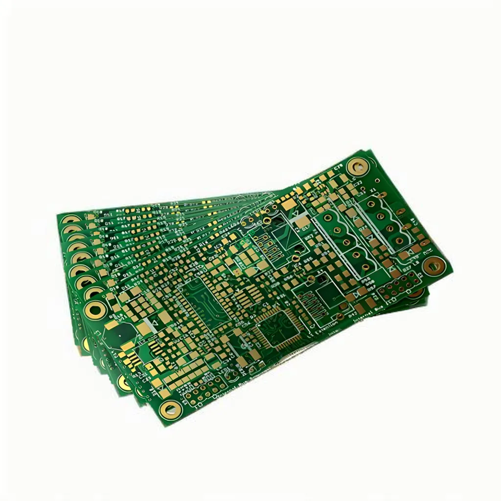
What is a 10Layers ENIG Board?
A 10-layer ENIG (Химическое никель, иммерсионное золото) board is an advanced многослойная печатная плата (печатная плата) with ten layers of conductive material, обычно медь, разделен изолирующими слоями. The “СОГЛАШАТЬСЯ” refers to the surface treatment applied to the copper traces, which involves electroless nickel and immersion gold plating. Этот тип печатная плата is designed for high-density and complex electronic applications.

Требования к дизайну
Designing a 10-layer ENIG board involves several key considerations:
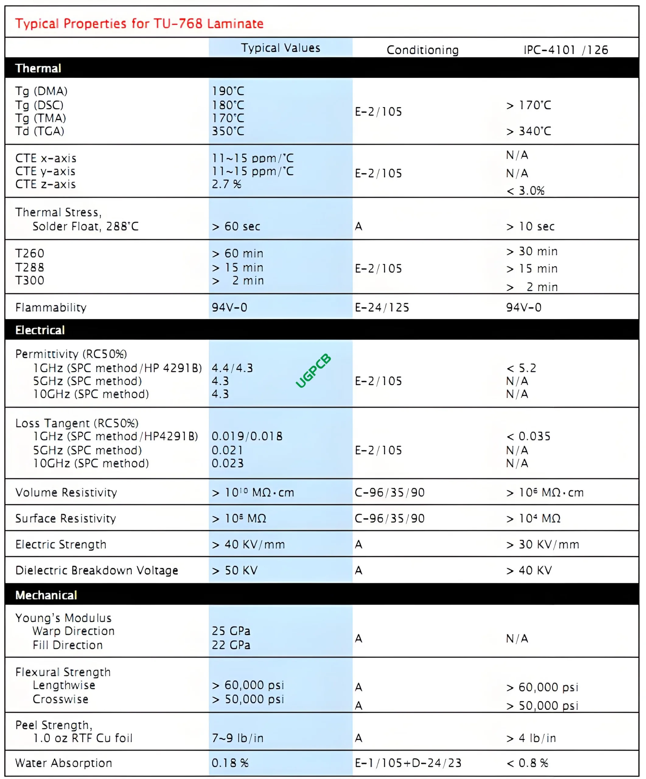
- Материал: Сделано из ТУ-768, a high-performance composite material known for its excellent electrical properties and durability.
- Количество слоев: Consists of ten layers, allowing for intricate and dense circuit designs.
- Толщина меди: Ranges from 2OZ to 3OZ, providing robust conductivity for high-power applications.
- Обработка поверхности: Features immersion gold plating, which offers excellent solderability and corrosion resistance.
- След и пространство: Minimum trace and space are set at 3mil (0.075мм), enabling fine details in the circuit design.
Как это работает?
The 10-layer ENIG board functions by providing multiple layers of conductive pathways, разделен изолирующими слоями, to interconnect electronic components. The immersion gold surface treatment ensures reliable soldering and long-term protection against oxidation and wear.
Приложения

Due to their complexity and reliability, 10-layer ENIG boards are widely used in various high-end electronic applications including:
- Aerospace and defense systems
- Высокоскоростное сетевое оборудование
- Advanced telecommunication devices
- Медицинское оборудование для визуализации
Классификация
10-layer ENIG boards can be classified based on several factors:
- Материалом: Most commonly made from TU-768 due to its balance of cost, сила, и электрические свойства.
- By Copper Thickness: Varies from lightweight (2ОЗ) to heavyweight (3ОЗ) depending on the application’s needs.
- По поверхности обработка: Features immersion gold plating, which provides excellent solderability and corrosion resistance.
Материалы используются
The primary materials used in manufacturing 10-layer ENIG boards include:
- ТУ-768: Армированный стекловолокном эпоксидный ламинат, обеспечивающий превосходную механическую прочность и термическую стабильность..
- Медь: Используется для проводящих слоев, толщина варьируется в зависимости от проектных требований.
- Припаяя маска: Обычно зеленый или белый, Он защищает медные следы от окисления и случайных коротких замыканий.
- Погружение Золото: Applied as a surface treatment to improve solderability and protect against corrosion.
Характеристики производительности
Key performance attributes of a 10-layer ENIG board include:
- Высокая плотность: Allows for more компоненты to be packed into a smaller area.
- Надежность: The use of multiple layers reduces the risk of electrical shorts and improves signal integrity.
- Целостность сигнала: Улучшено за счет более коротких путей прохождения сигнала и уменьшения перекрестных помех..
Структурная композиция
Структурно, a 10-layer ENIG board comprises:
- Проводящие слои: Изготовлен из меди, выгравированы в желаемые схемы.
- Изолирующие слои: Предотвратить электрические шорты между проводящими слоями.
- Plated Through-Hole Vias: Facilitate connections between different layers.
Отличительные особенности
Some notable features of a 10-layer ENIG board are:
- мелкий шаг: Allows for high-density interconnects making it ideal for compact devices.
- Надежность: The use of multiple layers provides a strong mechanical bond between the board and components.
- Универсальность: Подходит для широкого спектра применений благодаря настраиваемому количеству слоев и выбору материала..
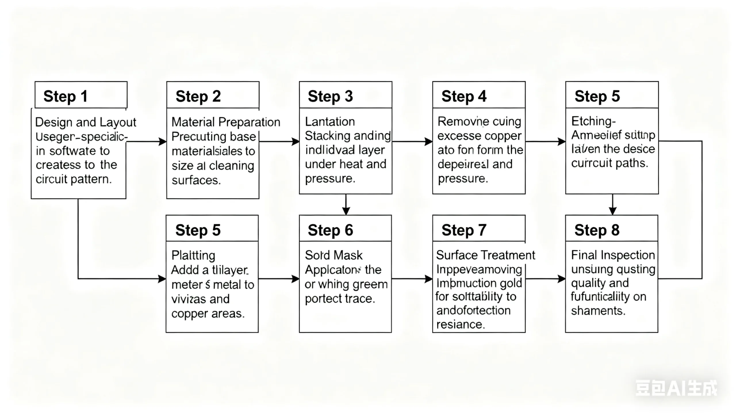
Производственный процесс
The manufacturing process of a 10-layer ENIG board involves several steps:
- Дизайн и макет: Использование специализированного программного обеспечения для создания шаблона схемы.
- Подготовка материала: Резка базовые материалы до размера и очистки поверхностей.
- Ламинирование: Упаковка и соединение отдельных слоев под теплом и давлением.
- Офорт: Удаление лишней меди для формирования желаемых путей цепи.
- Покрытие: Добавление тонкого слоя металла в VIAS и открытые медные зоны.
- Прикладная маска: Нанесение зеленого или белого покрытия для защиты следов.
- Обработка поверхности: Applying immersion gold for solderability and corrosion resistance.
- Заключительная проверка: Обеспечение качества и функциональности перед отправкой.
Варианты использования
Common scenarios where a 10-layer ENIG board might be employed include:
- High-density interconnect applications in aerospace and defense systems.
- Расширенные системы связи, требующие низкой потери сигнала.
- Портативные медицинские инструменты, нуждающиеся в надежной производительности в суровых условиях.
- Автомобильная электроника, требующая устойчивости и долговечности.
В итоге, the 10-layer ENIG board represents a significant advancement in printed circuit board technology offering unparalleled complexity and performance for modern electronic applications Its design flexibility combined with superior signal integrity and durability makes it an essential component in the development of next-generation high-end electronics and beyond


