
Overview of the 14 Слой тяжелая медная пласка катушка
The 14 Layer Heavy Copper Coil PCB is a high-density, Многослойная энергетическая плата, разработанная для приложений, требующих надежной электрической производительности и надежности. Этот печатная плата идеально подходит для сложных электронных систем, которые необходимы для управления высокой мощностью и целостностью сигнала.
Что такое 14 Слой тяжелая медная пласка катушка?
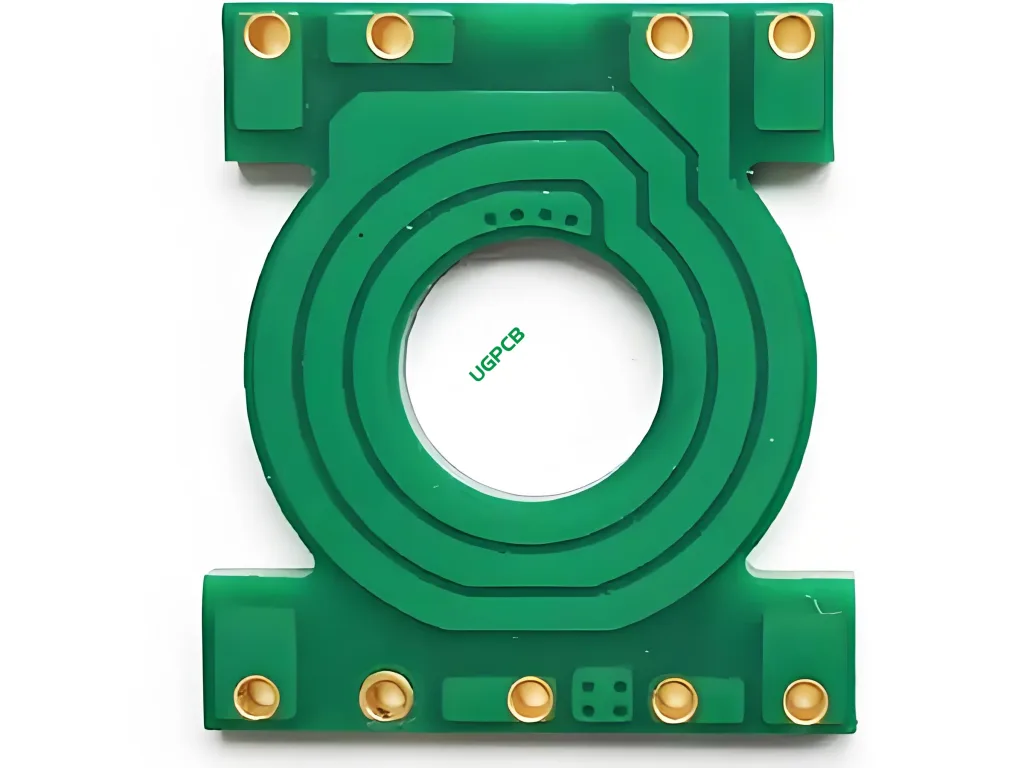
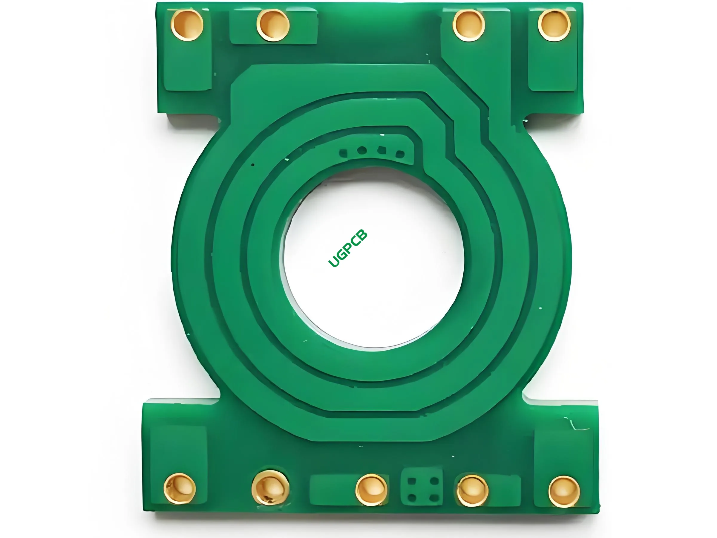
А 14 Layer Heavy Copper Coil PCB is a печатная плата (печатная плата) с 14 слои медных следов, каждое взвешивание 4 унции на квадратный фут. Этот тип печатной платы специально предназначен для приложений питания, где это необходимо для обработки больших токов и обеспечения стабильных электрических соединений.
Требования к дизайну
Требования к проектированию 14 Layer Heavy Copper Coil PCB are stringent to ensure its performance and reliability:
- Материал: EM827, выбрано для его превосходных электрических и тепловых свойств.
- Количество слоев: 14 слои для размещения сложных и плотных конструкций цепи.
- Цвет: Зеленый/белый для легкой идентификации и эстетической привлекательности.
- Готовая толщина: 4.0мм для обеспечения структурной целостности и долговечности.
- Толщина меди: 4Оз для обеспечения адекватной проводимости и рассеяния тепла.
- Обработка поверхности: Погружение золота для повышения припая и коррозионной устойчивости.
- Толщина меди в отверстии: 70Гм для лучшей электрической связи.
- Ширина линии: 0.3ММ для поддержки тонких схем.
- Минимальная апертура: 0.4ММ, чтобы обеспечить точное размещение компонентов.
Как это работает?
The 14 Layer Heavy Copper Coil PCB works by providing a platform for various electronic components to be interconnected through conductive pathways. Эти пути, или следы, изготовлены из меди и запечатлены на доске. Обработка поверхности погружения в погружение гарантирует, что эти следы остаются проводящими и устойчивыми к факторам окружающей среды.
Приложения
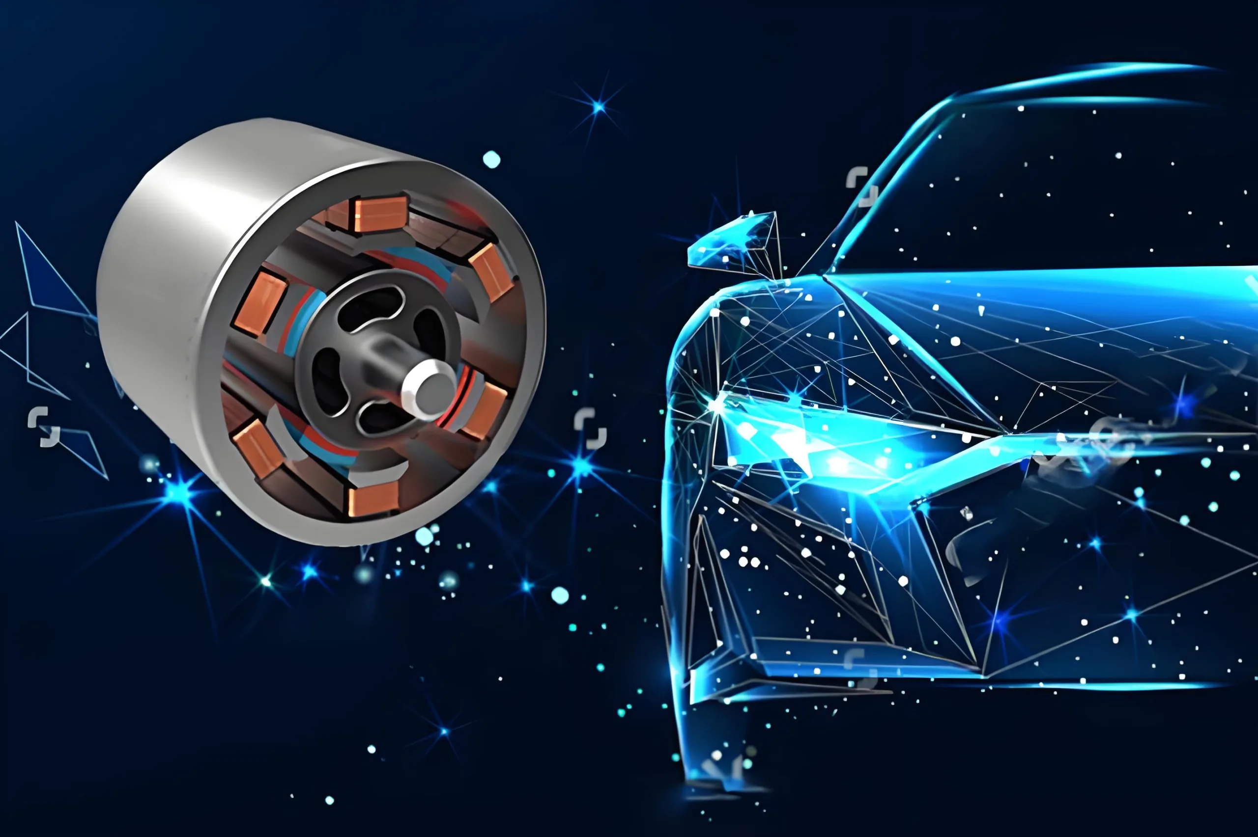
Основное применение средства 14 Layer Heavy Copper Coil PCB is in power electronics where it manages and regulates the flow of electrical power. Это включает в себя:
- Питания
- Моторные диски
- Возобновляемые энергетические системы
- Промышленные системы управления
Классификация
На основе его функций и приложений, а 14 Layer Heavy Copper Coil PCB can be classified as a high-power PCB designed for demanding power applications. Эта классификация подчеркивает его способность обрабатывать большие токи и обеспечивать стабильные электрические соединения.
Материальная композиция
Ядро материал используется в 14 Layer Heavy Copper Coil PCB is EM827, высокопроизводительный ламинат материал, известный своим превосходным механическим, тепло, и электрические свойства. Этот материал гарантирует, что печатная плата может противостоять требованиям электроэнергии.
Характеристики производительности
Эксплуатационные характеристики 14 Layer Heavy Copper Coil PCB include:
- Высокая мощность
- Отличная целостность сигнала
- Превосходное тепловое управление
- Надежная механическая прочность
- Долгосрочная стабильность
Структурные детали
Конструктивные детали 14 Layer Heavy Copper Coil PCB are as follows:
- Количество слоев: 14 слои
- Готовая толщина: 4.0мм
- Толщина меди: 4ОЗ
- Обработка поверхности: Погружение Золото
- Толщина меди в отверстии: 70ОДИН
- Ширина линии: 0.3мм
- Минимальная апертура: 0.4мм
Функции и преимущества
Основные особенности и преимущества 14 Layer Heavy Copper Coil PCB include:
- Взаимодействие высокой плотности
- Отличная способность обработки мощности
- Надежная механическая конструкция
- Надежная долгосрочная производительность
- Эстетические варианты цвета (Зеленый/Белый)
Производственный процесс
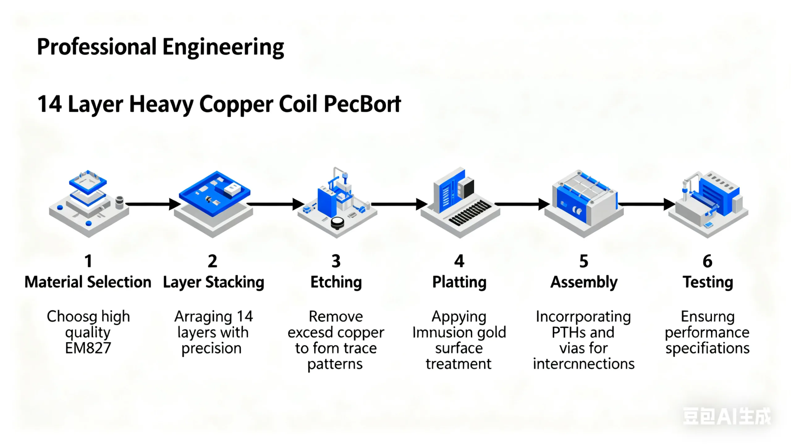
Производственный процесс 14 Layer Heavy Copper Coil PCB involves several steps, включая:
- Выбор материала: Выбор высококачественного материала EM827.
- Наложение слоев: Аранжировка 14 слои с точностью.
- Офорт: Удаление лишней меди, чтобы сформировать желаемые схемы трассировки.
- Покрытие: Применение обработки поверхности погружения в погружение.
- Сборка: Включение PTH и VIAS для взаимосвязей слоя.
- Тестирование: Обеспечение печатной платы соответствует всем спецификациям производительности.
Варианты использования
The 14 Layer Heavy Copper Coil PCB is used in various scenarios such as:
- Мощное промышленное оборудование
- Возобновляемые энергетические системы
- Контроллеры моторного привода
- Блоки питания


