
Высокопроизводительная двусторонняя печатная плата FR-4 Обзор продукта & Определение
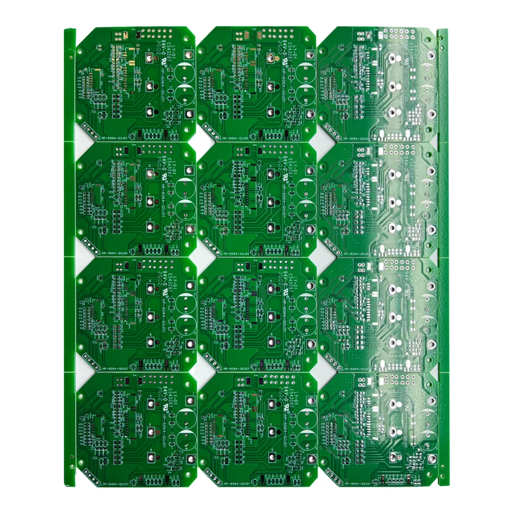
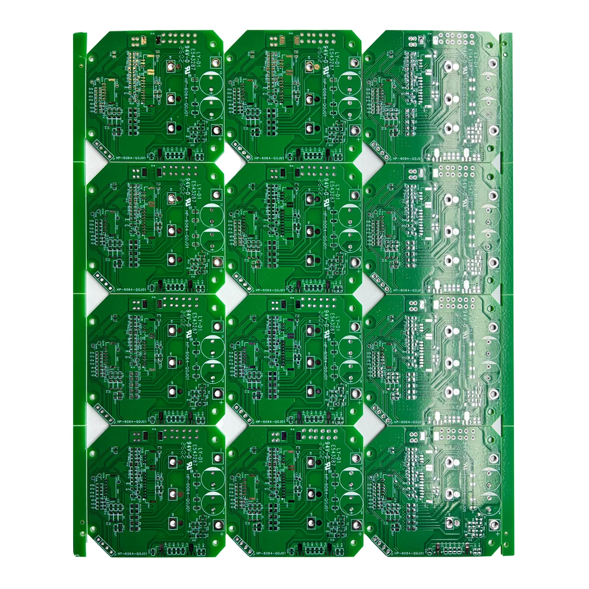
Этот 2-Слой жесткий Печатная плата (печатная плата) от UGPCB — это фундаментальное и широко используемое решение для электронных межсоединений.. Он имеет стандартный 1.6мм толщина доски, размеры 224.02мм х 189 мм, и использует высококачественные KB FR-4 ламинат. Эта двусторонняя печатная плата служит основным “позвоночник” для электронных конструкций, обеспечение надежных электрических соединений и механической поддержки компонентов. Это идеал, экономически эффективный выбор для широкого спектра промышленных систем управления, бытовая электроника, и приложения для электропитания.
Критические соображения дизайна
Успешный проект двусторонней печатной платы требует баланса электрических характеристик и технологичности.. Ключевые соображения включают в себя:
-
Стратегия маршрутизации: Эффективно используйте верхний и нижний уровни для маршрутизации трассировки.. Покрытые сквозные отверстия (PTH или переходные отверстия) включить межуровневые соединения. Тщательное планирование плотности трасс имеет решающее значение для предотвращения проблем с целостностью сигнала, таких как перекрестные помехи..
-
Дыра & Дизайн колодки: Укажите соответствующие размеры сверла и диаметры колодок для всех Переходные отверстия на печатной плате и выводы компонентов для обеспечения механической прочности и надежности пайки, придерживаясь Стандарты IPC для кольцевого кольца.
-
Власть & Наземные самолеты: Пока специальные самолеты отсутствуют, проектировщикам следует расширить трассы питания и заземления или реализовать медную заливку с сеткой, чтобы уменьшить импеданс и повысить стабильность — ключевой аспект надежной работы. дизайн печатной платы.
-
Проверка правил проектирования (ДРК): До изготовления, тщательно убедиться, что все параметры (ширина дорожки/просвет, размеры отверстий) соответствие возможностям производителя (согласно характеристикам этой платы) гарантировать Дизайн печатной платы для технологичности (DFM).
Принцип работы & Структура
Функциональность этого двухслойная плата обусловлено его слоистой структурой:
-
Строительство: Ядро состоит из Изолирующий диэлектрический слой ФР-4, облицованный медной фольгой (обычно 1 унция) с обеих сторон. Нежелательная медь вытравливается во время Изготовление печатной платы, формирование нужных схемных дорожек.
-
Электрическое соединение: Цепи на двух слоях соединены вертикально через Покрытые сквозные отверстия (ПТХ), созданный через механическое бурение с последующим Химическое и электролитическое осаждение меди.
-
Защита поверхности: The Выравнивание бессвинцовой пайкой горячим воздухом (ХАСЛ) Отделка, нанесенная на открытые медные площадки, предотвращает окисление и обеспечивает отличную паяемость при сборке компонентов..
Классификация продуктов & Материалы
По предоставленным характеристикам, этот продукт точно классифицируется следующим образом:
-
По количеству слоев: Двусторонняя печатная плата или 2-Слой платы.
-
По жесткости подложки: Жесткая печатная плата.
-
Базовым материалом: Печатная плата FR-4. Конкретно, ФР-4 из “КБ” бренд, ламинат из эпоксидного стекла, известный превосходной электроизоляцией, механическая прочность, и огнестойкость (УЛ94-В0).
-
По отделке поверхности: Бессвинцовая печатная плата HASL.
-
По сложности приложения: Стандартный, Универсальная печатная плата промышленного класса.
Производительность & Ключевые особенности
Использование указанных материалов и процессов, эта печатная плата обеспечивает следующие основные преимущества производительности:
-
Надежная механика & Электрические характеристики: The Материал КБ ФР-4 обеспечивает стабильную диэлектрическую проницаемость и низкий коэффициент рассеяния для целостности сигнала. Стандартная толщина 1,6 мм обеспечивает отличную устойчивость к изгибу и вибрации..
-
Надежные соединения: The Бессвинцовая поверхность HASL предоставляет квартиру, покрытие с высокой способностью к пайке, совместимое как с волновой, так и с ручной пайкой.
-
Превосходная термическая стабильность: Подложка FR-4 выдерживает стандартные температуры пайки и обеспечивает высокую постоянную рабочую температуру., подходит для большинства Промышленная электроника окружающая среда.
-
Высокая экономическая эффективность: По сравнению с многослойными платами, двусторонние печатные платы предлагают значительно ниже Стоимость изготовления печатной платы и более короткие сроки выполнения, представляет собой экономичное аппаратное решение.
-
Экологическое соответствие: The Бессвинцовый HASL процесс соответствует международным директивам, таким как RoHS.
Подробный производственный процесс
УГКПБ придерживается строгих, высокий стандарт Процесс изготовления печатной платы:
-
Инженерное дело & САМ: Анализ Gerber-файла, проверка ДФМ, и генерация фотоплота.
-
Панельизация: Резка большого ФР-4 ламинат с медным покрытием в производственные панели.
-
Бурение: Сверление отверстий для компонентов на станке с ЧПУ и Переходные отверстия на печатной плате.
-
Металлизация отверстий: Десмеар, химическое осаждение меди, и электролитическое меднение для образования проводящих Покрытые сквозные отверстия (ПТХ).
-
Узоры: Нанесение фоторезиста, контакт, разработка для переноса изображения схемы.
-
Офорт: Удаление ненужной меди для формирования точных дорожек цепи.
-
Припаяя маска & Шелковик: Нанесение паяльной маски LPI (обычно зеленый) и печать легенды.
-
Поверхностная отделка: Применение Бессвинцовый HASL покрытие открытых колодок.
-
Маршрутизация & Электрические испытания: Профилирование до окончательного контура платы и проведение электрических испытаний (Летающий зонд или испытание приспособления).
-
Заключительная проверка & Упаковка: Всесторонний Автоматическая оптическая проверка (АОИ), проверка размеров, и в вакуумной упаковке, влагонепроницаемая упаковка.
Основные приложения & Варианты использования
Эта спецификация двусторонней печатной платы FR-4 широко используется в надежный и экономичный приложения:
-
Промышленные системы управления: ПЛК-контроллеры, платы привода двигателя, интерфейсные модули датчиков.
-
Блоки питания: Импульсные источники питания (ИМПС), Системы ИБП, Платы драйверов светодиодов.
-
Бытовая электроника: Платы управления бытовой техникой (переменного тока, стиральные машины), контроллеры умного дома, аудио оборудование.
-
Автомобильная электроника: Модули управления кузовом (БЦМ), контроллеры освещения, некритичные информационно-развлекательные системы.
-
Телекоммуникационное оборудование: Функциональные модули в маршрутизаторах, переключатели.
-
Тест & Измерительные приборы: Панели сбора и отображения данных для оборудования.

Почему стоит выбрать UGPCB для нужд двусторонней печатной платы?
Сотрудничество с гарантиями УГКПБ:
-
Точное производство: Строгое соблюдение толщины 1,6 мм., 224.02размеры x189мм, и Материал ФР-4 спецификации.
-
Совершенство процессов: Стандартизированный Производство бессвинцовых печатных плат HASL обеспечивает стабильность и надежность от партии к партии.
-
Экспертная техническая поддержка: Наша команда оказывает всестороннюю поддержку, от дизайн печатной платы обзор на производственную консультацию.
-
Быстрая доставка под ключ: Мы предлагаем конкурентоспособные сроки выполнения стандартных двухслойных Прототипы печатных плат и производственные циклы.
Готовы начать ваш проект? Свяжитесь с UGPCB сегодня, чтобы получить конкурентоспособное предложение и экспертную поддержку.. Позвольте нам быть вашим доверенным лицом Производитель печатных плат и партнер для успеха.


