

Что такое 4 Слой платы?
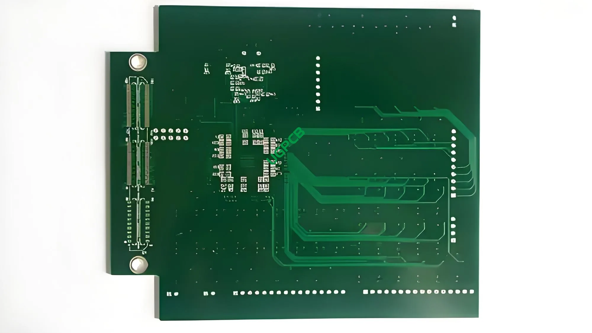
A 4-layer Printed Circuit Board (печатная плата) is an advanced электронный компонент that consists of four layers of conductive material, обычно медь, разделен изолирующими слоями. This multilayer structure allows for complex circuit designs with high density and improved performance.
Требования к дизайну
Designing a 4-layer PCB involves several key considerations:
- Материал: Commonly made from ФР-4, композитный материал, известный своими превосходными электрическими свойствами и доступностью..
- Количество слоев: Как следует из названия, it has four layers, which can handle more complex circuitry compared to single or double-sided boards.
- Толщина меди: Can range from 0.5OZ to 6OZ, depending on the application’s power requirements.
- Обработка поверхности: Опции включают иммерсионное золото., ОСП (Органическая припаяя консервант), and lead-free HASL (Heat Activated Solder Leveling), each offering different levels of solderability and protection.
- След и пространство: Minimum trace and space are typically set at 3mil (0.075мм), позволяющая учитывать мелкие детали в схемотехнике.
Как это работает?
The 4-layer PCB functions by providing a platform where electronic components can be mounted and interconnected using conductive pathways etched into the copper layers. These pathways are separated by insulating layers, preventing electrical shorts while allowing signals to pass through via plated through-holes or vias.
Приложения
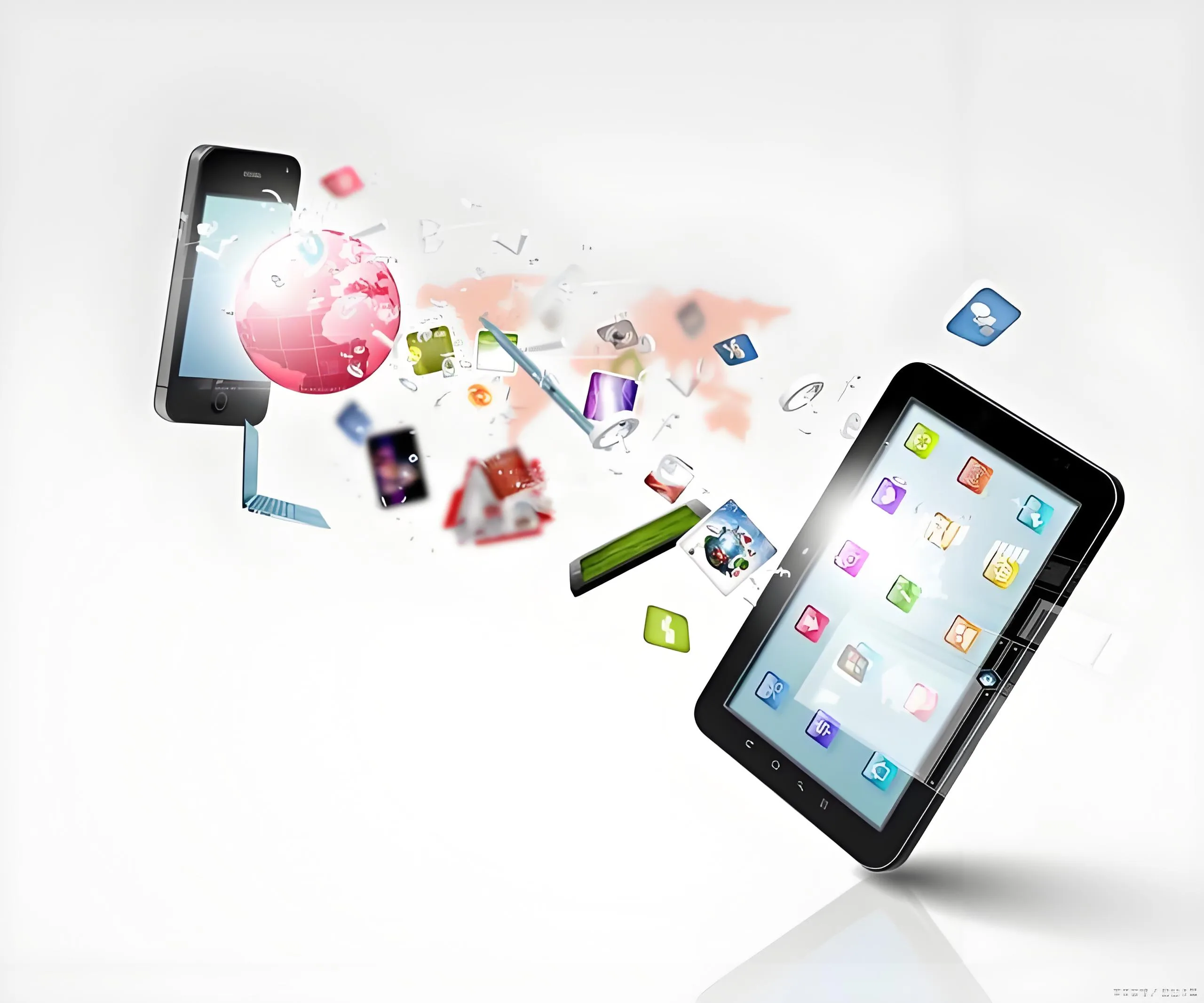
Due to their complexity and reliability, 4-слой печатные платы are widely used in various consumer electronics including:
- Смартфоны
- Таблетки
- Ноутбуки
- Gaming consoles
- High-end audio equipment
Классификация
4-layer PCBs can be classified based on several factors:
- Материалом: Чаще всего изготавливается из FR-4 из-за баланса стоимости., сила, и электрические свойства.
- By Copper Thickness: Varies from lightweight (0.5ОЗ) to heavyweight (6ОЗ) depending on the application’s needs.
- По поверхности обработка: Опции включают иммерсионное золото., ОСП, and lead-free HASL, каждый из них предлагает разные уровни защиты и паяемости.
Материалы используются
The primary materials used in manufacturing 4-layer PCBs include:
- ФР-4: Армированный стекловолокном эпоксидный ламинат, обеспечивающий превосходную механическую прочность и термическую стабильность..
- Медь: Используется для проводящих слоев, толщина варьируется в зависимости от проектных требований.
- Припаяя маска: Typically green, белый, красный, or black, Он защищает медные следы от окисления и случайных коротких замыканий.
- Surface Treatments: Such as immersion gold, ОСП, or lead-free HASL, which improve solderability and protect against corrosion.
Характеристики производительности
Key performance attributes of a 4-layer PCB include:
- Высокая плотность: Allows for more компоненты to be packed into a smaller area.
- Надежность: The use of multiple layers reduces the risk of electrical shorts and improves signal integrity.
- Целостность сигнала: Улучшено за счет более коротких путей прохождения сигнала и уменьшения перекрестных помех..
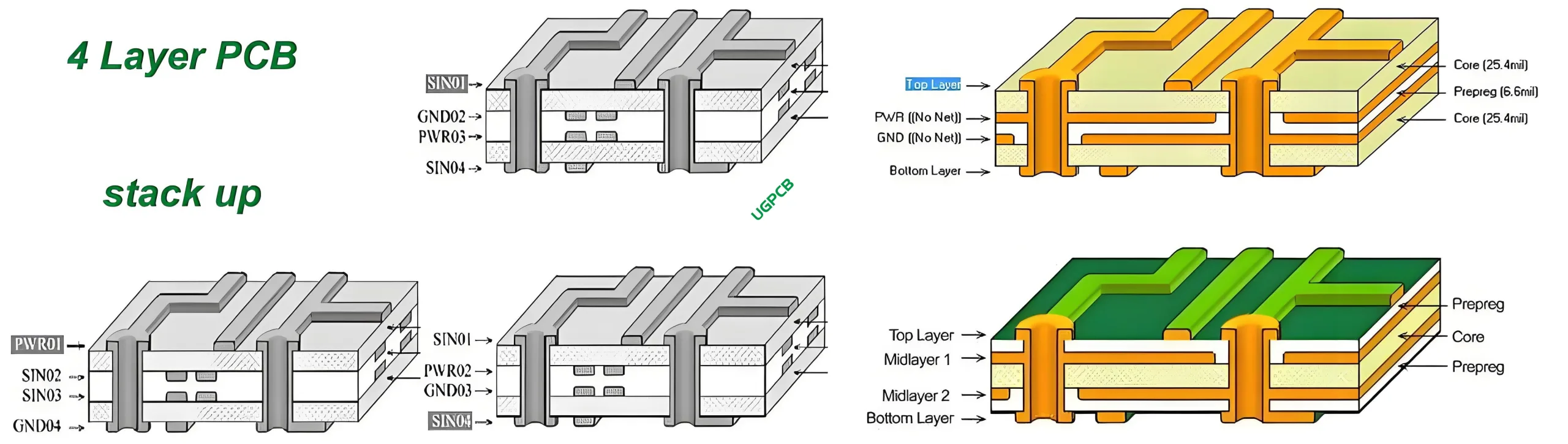
Структурная композиция
Структурно, a 4-layer PCB comprises:
- Проводящие слои: Изготовлен из меди, выгравированы в желаемые схемы.
- Изолирующие слои: Предотвратить электрические шорты между проводящими слоями.
- Plated Through-Hole Vias: Facilitate connections between different layers.
Отличительные особенности
Some notable features of a 4-layer PCB are:
- мелкий шаг: Обеспечивает высокую плотность межсоединений, что делает его идеальным для компактных устройств.
- Надежность: The use of multiple layers provides a strong mechanical bond between the board and components.
- Универсальность: Подходит для широкого спектра применений благодаря настраиваемому количеству слоев и выбору материала..
Производственный процесс
The manufacturing process of a 4-layer PCB involves several steps:
- Дизайн и макет: Использование специализированного программного обеспечения для создания шаблона схемы.
- Подготовка материала: Резка базовые материалы до размера и очистки поверхностей.
- Ламинирование: Упаковка и соединение отдельных слоев под теплом и давлением.
- Офорт: Удаление лишней меди для формирования желаемых путей цепи.
- Покрытие: Добавление тонкого слоя металла в VIAS и открытые медные зоны.
- Прикладная маска: Applying the green, белый, красный, or black coating to protect traces.
- Обработка поверхности: Applying immersion gold, ОСП, or lead-free HASL for solderability.
- Заключительная проверка: Обеспечение качества и функциональности перед отправкой.
Варианты использования
Common scenarios where a 4-layer PCB might be employed include:
- Приложения для взаимодействия с высокой плотностью в мобильных устройствах.
- Расширенные системы связи, требующие низкой потери сигнала.
- Портативные медицинские инструменты, нуждающиеся в надежной производительности в суровых условиях.
- Автомобильная электроника, требующая устойчивости и долговечности.
В итоге, the 4-layer PCB represents a significant advancement in печатная плата технология, Предлагая непревзойденную сложность и производительность для современных электронных применений. Its design flexibility combined with superior signal integrity and durability makes it an essential component in the development of next-generation consumer electronics and beyond.


