
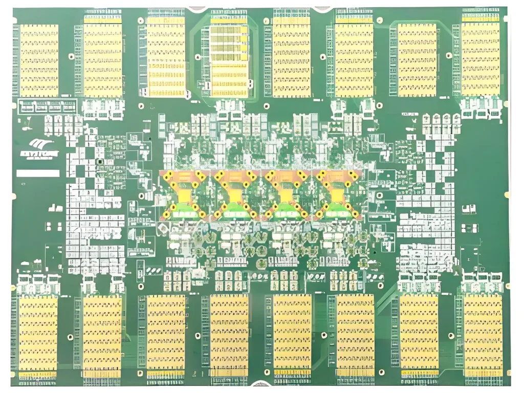
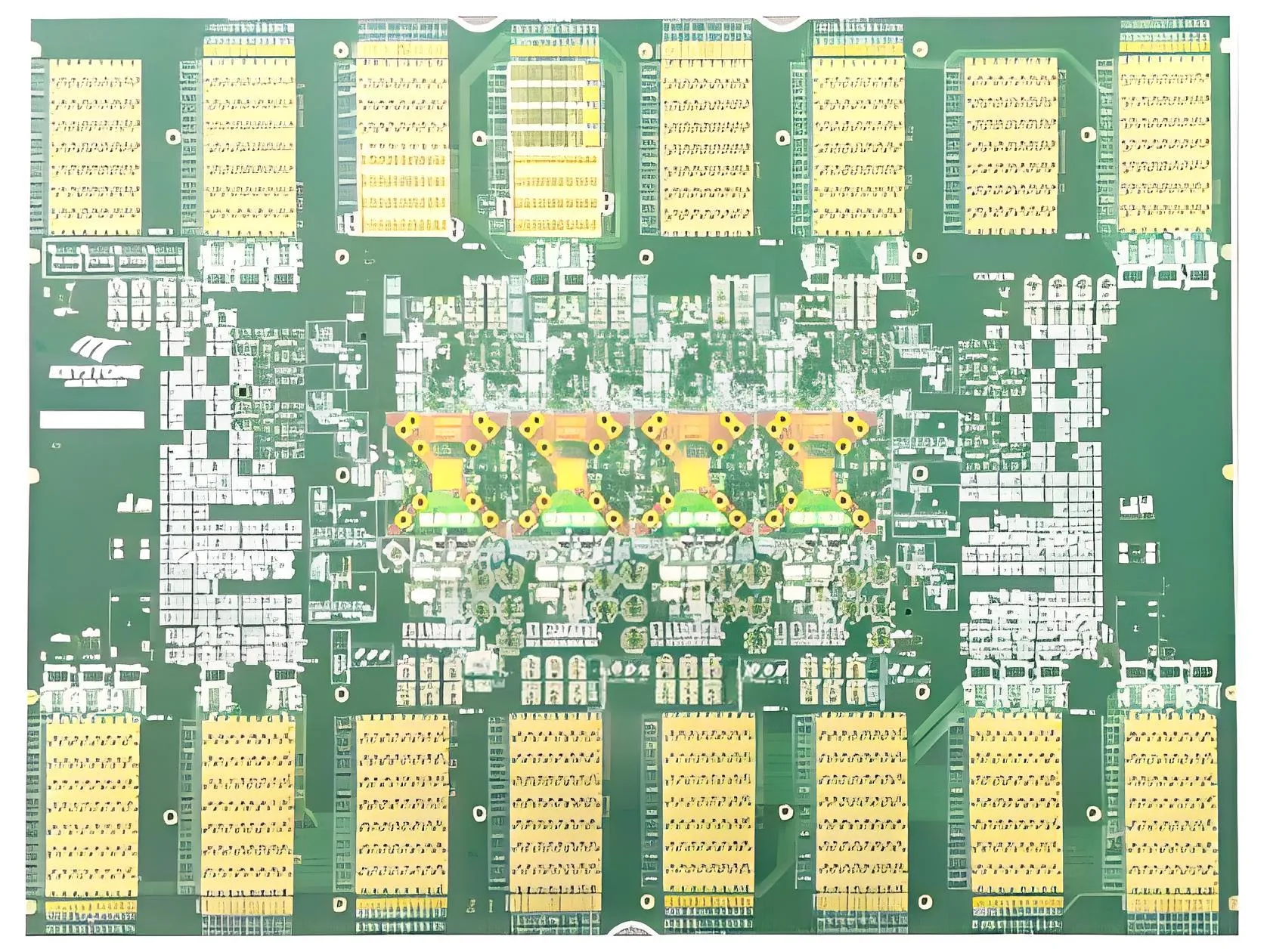
Overview of the 62-Layer ATE Load PCB
The 62-Layer ATE Load PCB is a high-performance, ultra-high-density печатная плата engineered for Automated Test Equipment (ЕЛ) системы. Designed to handle complex signal routing and high-power loads, it meets rigorous testing requirements in semiconductor manufacturing and advanced electronics validation.
Key Definition
An ATE Load PCB is a specialized circuit board that simulates real-world operating conditions for testing integrated circuits (ICS) и электронные компоненты. The 62-layer configuration supports intricate signal paths, Распределение энергии, and thermal management in compact designs.
Critical Design Parameters
-
Количество слоев: 62 layers for multi-domain signal isolation and power plane optimization.
-
Размеры: 16.9″ × 22.9″ (large format for multi-device integration).
-
Толщина: 250 мил (balances rigidity and thermal dissipation).
-
Материал: FR4 Htg (high-temperature glass epoxy for stability up to 180°C).
-
Минимальный размер отверстия: 8 мил (supports high-density interconnects).
-
BGA Pitch: 0.65мм (enables fine-pitch component mounting).
-
Соотношение сторон: 32:1 (ensures reliable plating in microvias).
-
Drill-to-Copper: 7 мил (prevents short circuits).
-
Пофв & Back-Drilling: Eliminates signal distortion in high-frequency applications.
-
Поверхностная отделка: Энэг (Electroless Nickel Electroless Gold for corrosion resistance).
Core Functionality
The печатная плата routes test signals between ATE systems and devices under test (DUTs), ensuring accurate voltage/current measurements. Back-drilling removes unused via stubs to minimize signal reflections, while POFV (Plated Over Filled Vias) enhances thermal conductivity and structural integrity.
Основные приложения
-
Полупроводниковое тестирование: Validates ICs, процессоры, and memory modules.
-
Аэрокосмическая промышленность & Оборона: Mission-critical avionics and radar systems.
-
Telecom Infrastructure: High-speed data transmission equipment.
-
Медицинские устройства: Precision diagnostic and imaging tools.
Material Advantages
FR4 HTg provides:
-
Тепловая устойчивость: Stable performance under cyclic thermal stress.
-
Низкие диэлектрические потери: Critical for high-frequency signal integrity.
-
Механическая прочность: Resists warping during multilayer lamination.
Структурные особенности
-
Hybrid Stackup: Combines high-speed, власть, и грунтовые слои.
-
Технология микровий: Laser-drilled microvias (8 мил) enable dense interlayer connections.
-
Controlled Impedance Traces: Minimizes crosstalk in 0.65mm BGA layouts.
Performance Highlights
-
Целостность сигнала: <3% insertion loss at 10 ГГц.
-
Power Handling: Supports 20A per power plane.
-
Тепловое управление: 1.2 W/mK thermal conductivity via POFV.
Производственный рабочий процесс
-
Material Prep: Cut FR4 HTg cores and prepreg sheets.
-
Лазерное сверление: Create 8-mil microvias with ±1 mil tolerance.
-
Покрытие & Пофв: Electroplate vias and fill with conductive epoxy.
-
Back-Drilling: Remove excess via stubs using depth-controlled drills.
-
Ламинирование: Press 62 layers under high temperature/pressure.
-
Поверхностная отделка: Apply ENEG for solderability and oxidation resistance.
-
Тестирование: Validate impedance, continuity, and thermal cycling.
Ideal Use Cases
-
High-Frequency ATE Systems: Tests 5G RF components and millimeter-wave devices.
-
Multi-Site Testing: Parallel validation of 16+ DUTs on a single board.
-
Суровые условия: Oil/gas exploration sensors and automotive ECU testing.


