

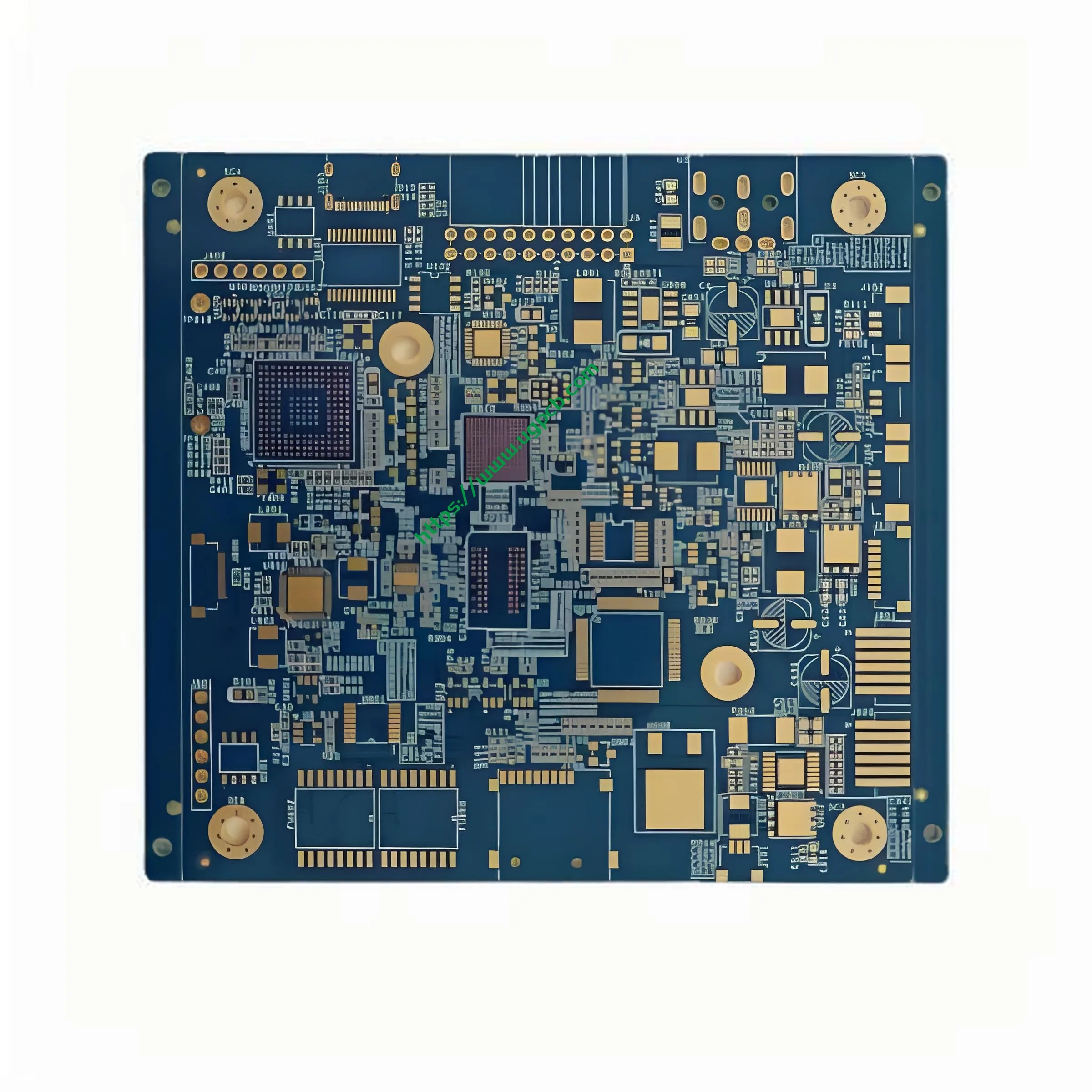
What is a 6L 1+N+1 HDI PCB?
A 6L 1+N+1 HDI PCB stands for a six-layer High Density Interconnect (ИЧР) печатная плата, featuring one core layer flanked by N signal layers and another core layer. This configuration allows for high density interconnections, making it suitable for advanced electronic applications. The “1+N+1” designation refers to the arrangement of the core layers and signal layers.
Требования к дизайну
The design of a 6L 1+N+1 HDI PCB requires careful consideration of several factors:
- Наложение слоев: Proper alignment of the core and signal layers to ensure optimal electrical performance.
- След и пространство: Minimal trace width and space of 3mil/3mil to accommodate fine features.
- Hole Sizes: Mechanical holes as small as 0.2mm and laser holes down to 0.1mm for precise component placement.
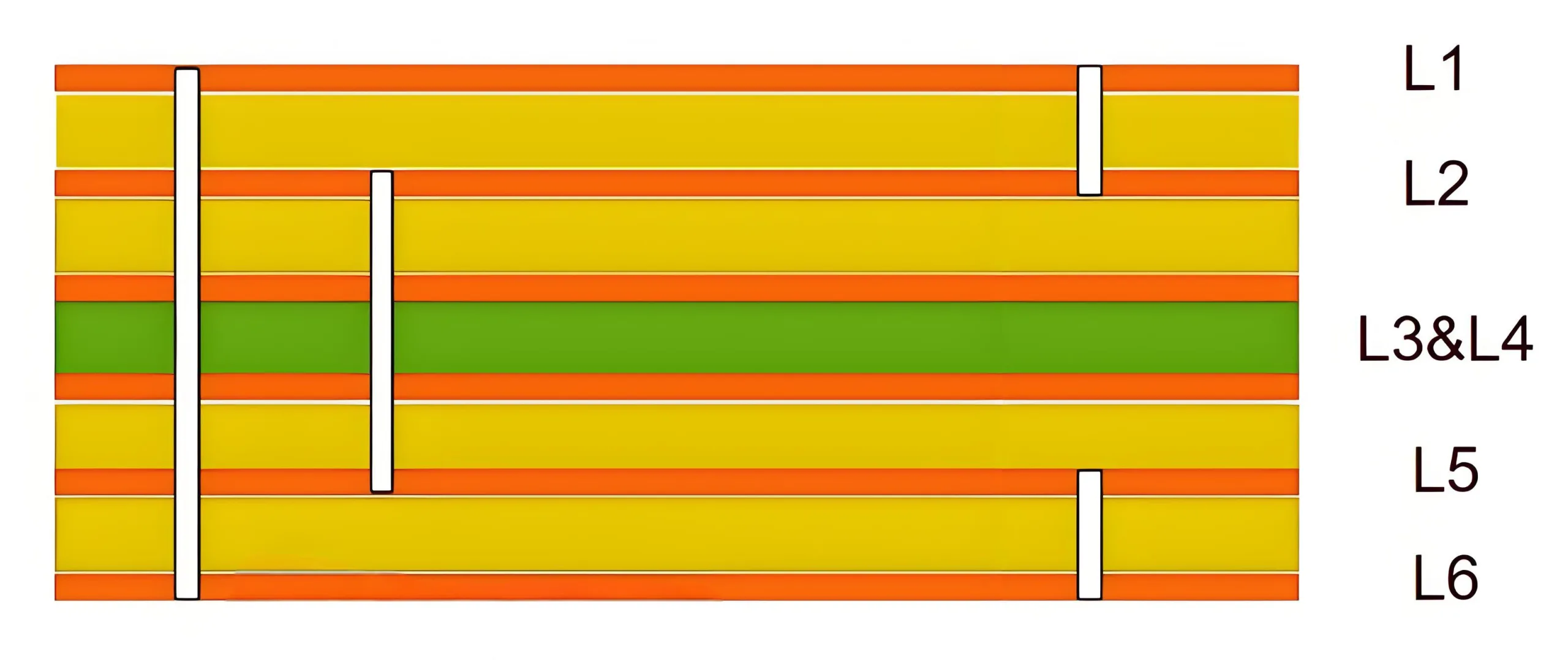
- Толщина меди: Varied copper thickness with inner layers at 1OZ and outer layers at 0.5OZ to balance conductivity and flexibility.
Как это работает?
The functionality of a 6L 1+N+1 HDI печатная плата relies on its multilayer structure and the use of high-density interconnects. Each layer serves a specific purpose:
- Core Layers: Provide structural integrity and act as the foundation for signal layers.
- Signal Layers: Carry electrical signals between components.
- Обработка поверхности погружения в погружение: Ensures excellent solderability and long-term reliability by preventing oxidation.
Приложения и классификации
Эти печатные платы are primarily used in intelligent digital products where compact size and high performance are crucial. They can be classified based on their complexity and the number of layers, with the 6L 1+N+1 configuration being highly versatile for various applications.
Материалы и производительность
Constructed from ФР-4 (ИТЕК), these PCBs offer excellent thermal stability and mechanical strength. Зеленая/белая цветовая схема способствует визуальному осмотре и устранению неполадок. The finished thickness of 1.0mm provides a robust yet flexible board suitable for intricate designs.
Структура и особенности
The unique structure of a 6L 1+N+1 HDI PCB includes:
- Шесть слоев: One core layer, N сигнальных слоев, and another core layer.
- High Density Interconnects: Allow for complex routing and minimal space usage.
- Погружение золота: Enhances conductivity and protects against corrosion.
Производственный процесс
The manufacturing process involves several sophisticated steps:
- Подготовка материала: Selecting high-quality FR-4 substrate and copper foils.
- Наложение слоев: Arranging the layers in a precise order to achieve the desired “1+N+1” configuration.
- Склеивание: Использование тепла и давления для соединения слоев вместе..
- Офорт: Нанесение травителя для удаления излишков меди, оставляя только желаемые проводящие пути.
- Покрытие: Adding a thin layer of metal to improve conductivity and solderability.
- Обработка поверхности: Applying immersion gold to protect against oxidation and enhance solderability.
- Контроль качества: Проведение тщательных проверок и испытаний для обеспечения соответствия каждой доски строгим стандартам качества..

Варианты использования и сценарии
6L 1+N+1 HDI PCBs are ideal for use in intelligent digital products where miniaturization and high performance are critical. Общие приложения включают в себя:
- Смартфоны: Создание более тонких конструкций без ущерба для функциональности и производительности..
- Таблетки: Обеспечение надежного подключения для высокоскоростной передачи и обработки данных..
- Носимые устройства: Поддержка компактных конструкций при сохранении высокой производительности и долговечности..


