

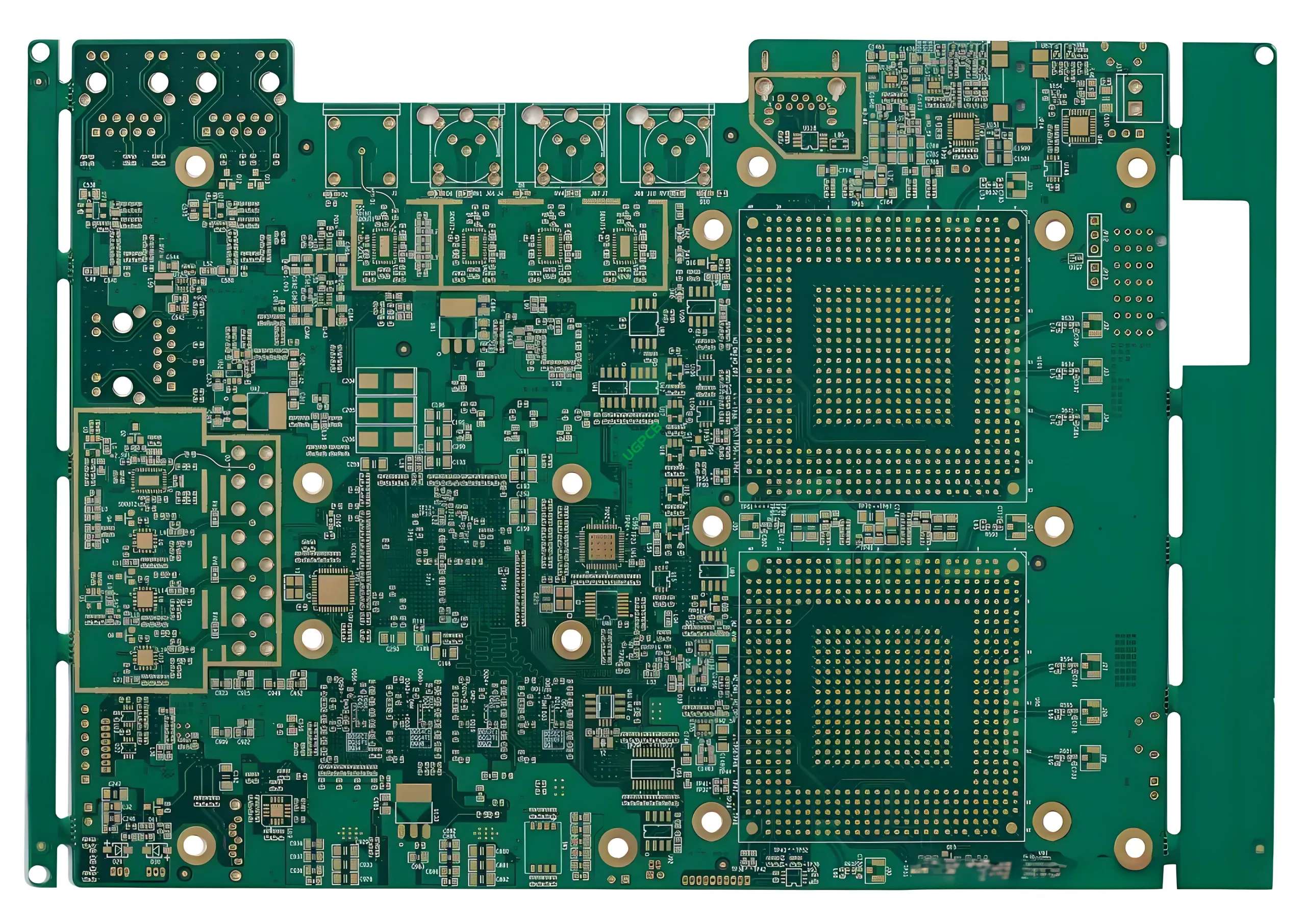
Что такое печатная плата BGA?
Массив шариковой сетки (БГА) Печатная плата (печатная плата) это тип монтажная плата с сеткой из шариков припоя на нижней стороне, используется для подключения электронные компоненты к доске. Такая конструкция обеспечивает более высокую плотность входных/выходных соединений и улучшенные электрические характеристики по сравнению с традиционными технологиями сквозного или поверхностного монтажа. (СМТ) печатные платы.
Требования к дизайну
Проектирование печатной платы BGA включает в себя несколько ключевых моментов.:
- Материал: Обычно изготавливается из ФР-4, композитный материал, известный своими превосходными электрическими свойствами и доступностью..
- Количество слоев: Многослойные конструкции распространены, предоставление большего места для сложных схем.
- Толщина меди: Обычно указывается как 1/1 унции, баланс проводимости с экономической эффективностью.
- Обработка поверхности: Часто включает иммерсионное золото для улучшения паяемости и защиты от окисления..
- След и пространство: Минимальная трассировка и пространство обычно устанавливаются на уровне 4 мил., позволяющая учитывать мелкие детали в схемотехнике.
Как это работает?
Печатная плата BGA обеспечивает платформу, на которой можно монтировать и соединять электронные компоненты с помощью сетки шариков припоя.. Эти шары выстроены в узор на нижней стороне доски., соответствует контактным площадкам на компоненте. При применении тепла, припой плавится и создает прочную связь, обеспечение надежных электрических соединений.
Приложения
Благодаря высокой плотности и надежности, Печатные платы BGA широко используются в различных электронных продуктах, включая:
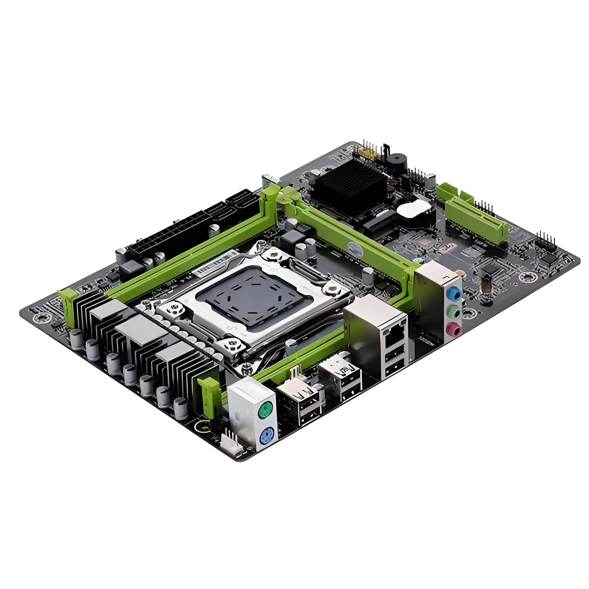
- Компьютерные материнские платы
- Высокопроизводительные серверы
- Сетевое оборудование
- Передовая бытовая электроника, такая как игровые консоли и интеллектуальные устройства.
Классификация
Печатные платы BGA можно классифицировать по нескольким факторам.:
- Материалом: Чаще всего изготавливается из FR-4 из-за баланса стоимости., сила, и электрические свойства.
- По количеству слоев: Может варьироваться от двусторонней до многослойной конфигурации., в зависимости от сложности схемы.
- По поверхности обработка: Опции включают иммерсионное золото., истекать кровью, или органические консерванты для пайки (ОСП), каждый из них предлагает разные уровни защиты и паяемости.
Материалы используются
Первичный материалы используемые при производстве печатных плат BGA, включают:
- ФР-4: Армированный стекловолокном эпоксидный ламинат, обеспечивающий превосходную механическую прочность и термическую стабильность..
- Медь: Используется для проводящих слоев, толщина варьируется в зависимости от проектных требований.
- Припаяя маска: Обычно зеленый или белый, Он защищает медные следы от окисления и случайных коротких замыканий.
- Погружение Золото: Обработка поверхности, улучшающая паяемость и защищающая от коррозии..
Характеристики производительности
Ключевые характеристики производительности печатной платы BGA включают в себя:
- Высокая плотность: Позволяет разместить больше компонентов на меньшей площади..
- Надежность: Использование шариков припоя снижает риск механического повреждения из-за вибрации или удара..
- Целостность сигнала: Улучшено за счет более коротких путей прохождения сигнала и уменьшения перекрестных помех..
Структурная композиция
Структурно, Печатная плата BGA содержит:
- Проводящие слои: Изготовлен из меди, выгравированы в желаемые схемы.
- Изолирующие слои: Предотвратить электрические шорты между проводящими слоями.
- Шарики для припоя: Расположены в виде сетки на нижней стороне платы для крепления компонентов..
Отличительные особенности
Некоторые примечательные особенности печатной платы BGA::
- мелкий шаг: Обеспечивает высокую плотность межсоединений, что делает его идеальным для компактных устройств.
- Надежность: Использование шариков припоя обеспечивает прочную механическую связь между платой и компонентами..
- Универсальность: Подходит для широкого спектра применений благодаря настраиваемому количеству слоев и выбору материала..
Производственный процесс
Процесс производства печатной платы BGA включает в себя несколько этапов.:
- Дизайн и макет: Использование специализированного программного обеспечения для создания шаблона схемы.
- Подготовка материала: Резка базовые материалы до размера и очистки поверхностей.
- Ламинирование: Упаковка и соединение отдельных слоев под теплом и давлением.
- Офорт: Удаление лишней меди для формирования желаемых путей цепи.
- Покрытие: Добавление тонкого слоя металла в VIAS и открытые медные зоны.
- Прикладная маска: Нанесение зеленого или белого покрытия для защиты следов.
- Обработка поверхности: Нанесение иммерсионного золота или другой обработки для улучшения паяемости..
- Заключительная проверка: Обеспечение качества и функциональности перед отправкой.
Варианты использования
Общие сценарии использования печатной платы BGA включают в себя::
- Приложения для взаимодействия с высокой плотностью в мобильных устройствах.
- Расширенные системы связи, требующие низкой потери сигнала.
- Портативные медицинские инструменты, нуждающиеся в надежной производительности в суровых условиях.
- Автомобильная электроника, требующая устойчивости и долговечности.
В итоге, Печатная плата BGA представляет собой значительный прогресс в технологии печатных плат., Предлагая непревзойденную сложность и производительность для современных электронных применений. Его гибкость дизайна, в сочетании с превосходной целостностью сигнала и долговечностью, делает его важным компонентом в разработке электронных продуктов следующего поколения и за его пределами.


