
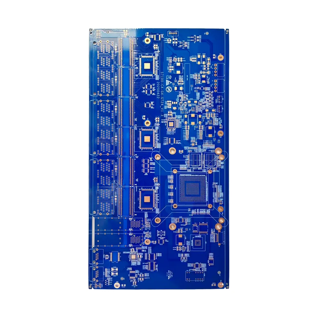

Overview of the Blue Solder Mask PCB
The Blue Solder Mask PCB is a high-density, multilayer printed circuit boarдюймовый (печатная плата) designed for digital applications requiring mass production. Этот печатная плата идеально подходит для сложных электронных систем, которые необходимы для управления высокой мощностью и целостностью сигнала.

What is a Blue Solder Mask PCB?
A Blue Solder Mask PCB is a printed circuit board (печатная плата) with a blue solder mask layer, which is used to protect the copper traces from oxidation and short circuits. The blue color makes it easy to distinguish different компоненты and layers during assembly and inspection.
Требования к дизайну
The design requirements for a Blue Solder Mask PCB are stringent to ensure its performance and reliability:
- Материал: ФР4, выбрано для его превосходных электрических и тепловых свойств.
- Количество слоев: 6 слои для размещения сложных и плотных конструкций цепи.
- Цвет: Синий/белый для легкой идентификации и эстетической привлекательности.
- Готовая толщина: 1.2мм для обеспечения структурной целостности и долговечности.
- Толщина меди: 1/0.5/0.5/0.5/0.5/1 Оз для обеспечения адекватной проводимости и рассеяния тепла.
- Обработка поверхности: Погружение золота для повышения припая и коррозионной устойчивости.
- Минимальная трассировка и пространство: 4мил(0.1мм) для поддержки тонких схем схемы.
Как это работает?
The Blue Solder Mask PCB works by providing a platform for various electronic components to be interconnected through conductive pathways. Эти пути, или следы, изготовлены из меди и запечатлены на доске. The blue solder mask layer protects the copper traces from environmental factors, В то время как обработка поверхности погружения в погружение гарантирует, что эти следы остаются проводящими и устойчивыми к коррозии.
Приложения
The primary application of the Blue Solder Mask PCB is in digital electronics where it manages and regulates the flow of electrical signals. Это включает в себя:
- Digital signal processors
- Микроконтроллеры
- Memory modules
- Устройства передачи данных
Классификация
На основе его функций и приложений, the Blue Solder Mask PCB can be classified as a high-speed digital PCB designed for mass production. Эта классификация подчеркивает его способность обрабатывать высокочастотные сигналы и обеспечивать стабильные электрические соединения.
Материальная композиция
Ядро материал used in the Blue Solder Mask PCB is FR4, высокопроизводительный композитный материал, известный своим превосходным механическим, тепло, и электрические свойства. This material ensures that the PCB can withstand the demands of digital applications.
Характеристики производительности
The performance characteristics of the Blue Solder Mask PCB include:
- Высокая целостность сигнала
- Низкая потеря сигнала
- Превосходное тепловое управление
- Надежная механическая прочность
- Долгосрочная стабильность
Структурные детали
The structural details of the Blue Solder Mask PCB are as follows:
- Количество слоев: 6 слои
- Готовая толщина: 1.2мм
- Толщина меди: 1/0.5/0.5/0.5/0.5/1 ОЗ
- Обработка поверхности: Погружение Золото
- Минимальная трассировка и пространство: 4мил(0.1мм)
Функции и преимущества
The key features and benefits of the Blue Solder Mask PCB include:
- Взаимодействие высокой плотности
- Отличная целостность сигнала
- Надежная механическая конструкция
- Надежная долгосрочная производительность
- Эстетические варианты цвета (Синий/Белый)
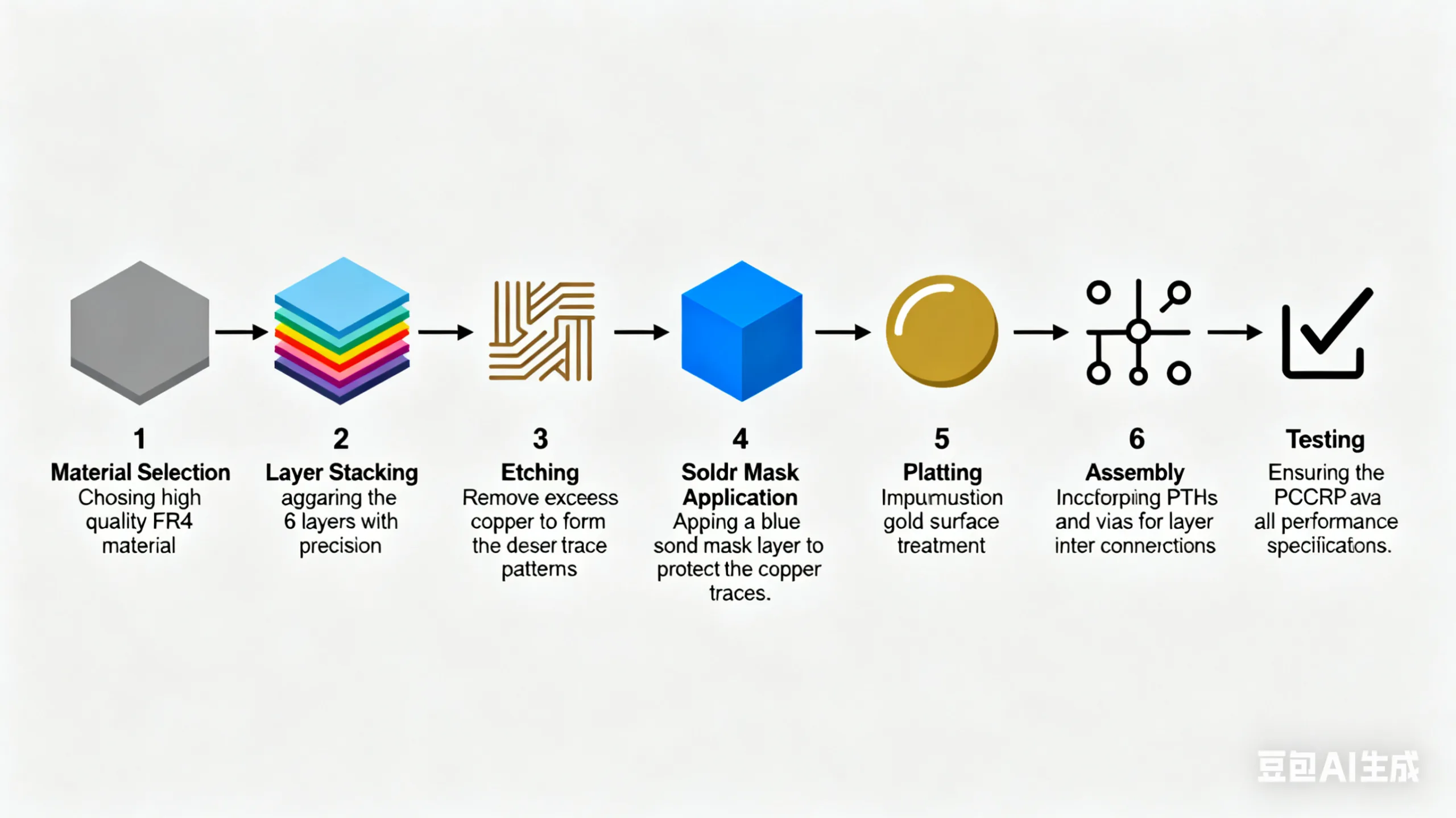
Производственный процесс
The production process of the Blue Solder Mask PCB involves several steps including:
- Выбор материала: Choosing high-quality FR4 material.
- Наложение слоев: Аранжировка 6 слои с точностью.
- Офорт: Удаление лишней меди, чтобы сформировать желаемые схемы трассировки.
- Прикладная маска: Applying a blue solder mask layer to protect the copper traces.
- Покрытие: Применение обработки поверхности погружения в погружение.
- Сборка: Включение PTH и VIAS для взаимосвязей слоя.
- Тестирование: Обеспечение печатной платы соответствует всем спецификациям производительности.
Варианты использования
The Blue Solder Mask PCB is used in various scenarios such as:
- Digital consumer electronics
- Промышленные системы управления
- Telecommunication equipment
- Автомобильная электроника


I gotta favorite this site it seems extremely helpful handy