

Знакомство с двухсторонней печатной платой UGPCB для релейной защиты
УГКПБ специализируется на производстве высокопроизводительных двусторонний печатные платы (печатные платы) специально для систем релейной защиты. Эти печатные платы разработаны с использованием Эпоксидная стеклоткань ФР-4 как базовый материал, обеспечение превосходной электрической изоляции и механической прочности.. Имеет конечную толщину 1,6 мм и толщину меди 1 унцию. (примерно 35 мкм), эти платы поддерживают надежную токопроводящую способность. The ОСП (Органическая припаяя консервант) обработка поверхности улучшает паяемость, защищая медные площадки от окисления. С минимальным следом и интервалом 8 мил. (0.2мм), Конструкции UGPCB обеспечивают оптимальную целостность сигнала для приложений прецизионной релейной защиты.. Доступен как в черном, так и в белом цветах паяльной маски., эти печатные платы соответствуют Стандарты CTI600, предлагая высокий сравнительный индекс отслеживания для предотвращения электрических сбоев во влажных условиях.
Что такое двухсторонняя печатная плата?
А Двусторонняя печатная плата включает в себя проводящие медные слои с обеих сторон изолирующей подложки, такой как ФР-4. Слои соединяются между собой с помощью металлизированные сквозные отверстия (ПТХ) или переходные отверстия, создание сложных схем в компактной форме. В отличие от односторонних печатных плат, двусторонние варианты обеспечивают более высокую плотность компонентов и гибкость компоновки, что делает их идеальными для устройств средней сложности, таких как системы релейной защиты.. Эти платы поддерживают двусторонняя сборка, включая технологии сквозного и поверхностного монтажа (СМТ), и широко используются в промышленности, телекоммуникации, и автомобильная электроника.
Рекомендации по проектированию печатных плат релейной защиты
-
Ширина следа и расстояние: УГКПБ рекомендует минимум 8мил (0.2мм) для ширины дорожки и расстояния для снижения риска короткого замыкания и обеспечения четкости сигнала в средах с высоким напряжением .
-
Термальные подушечки: Использовать заштрихованные термопрокладки для больших площадей меди для отвода тепла во время пайки, снижение риска виртуальных суставов .
-
Через спецификации: Для надежных межслойных соединений, укажите PTH с минимальным диаметром готового отверстия 0,3 мм и кольцевым кольцом 0,7 мм или больше. .
-
Медные плоскости с решеткой: Используйте сетчатые заземляющие плоскости с интервалом ≥10 мил, чтобы минимизировать деформацию печатной платы во время пайки волновой пайкой. .
-
Детали паяльной маски: Точно определите отверстия паяльной маски, используя слой паяльной маски в файлах дизайна, чтобы предотвратить перемычки и обнажить термопрокладки. .
Как двусторонние печатные платы работают в релейной защите
В системах релейной защиты, двусторонние печатные платы функционируют как центральная нервная система, контроль электрических параметров и инициирование отключения при неисправностях. Двухуровневая компоновка облегчает интеграцию датчики тока, микропроцессоры, и модули связи. Например, дорожки на верхнем слое могут нести низковольтные управляющие сигналы, в то время как нижний уровень обрабатывает сильноточные пути. Нанесенные сквозными отверстиями создавать низкоомные соединения между слоями, обеспечение быстрого обнаружения неисправностей и реагирования на них. The Подложка с рейтингом CTI600 сопротивляется проводящей анодной нити (Каф) формирование, что имеет решающее значение для долговечности в условиях высокой влажности.
Применение печатных плат релейной защиты UGPCB
Двусторонние печатные платы UGPCB используются в:
-
Релейные системы электросетей: Для защиты от перегрузки по току и замыкания на землю.
-
Промышленные панели управления: Мониторинг оборудования на производственных предприятиях.
-
Инверторы возобновляемой энергии: Защита преобразователей солнечной/ветровой энергии.
-
Телекоммуникационная инфраструктура: Защита источников питания базовой станции.
-
Системы железнодорожной сигнализации: Обеспечение безаварийного переключения путей.
Классификация двусторонних печатных плат
-
Материалом: ФР-4 (стандартный), СЕМ-3 (средний уровень), и полиимид (высокотемпературная).
-
По отделке поверхности: ОСП (По умолчанию UGPCB), ХАСЛ, СОГЛАШАТЬСЯ, и иммерсионная банка.
-
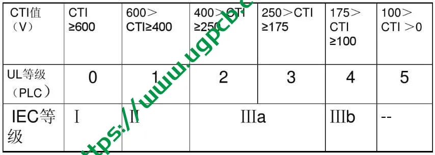
По рейтингу CTI: CTI600 (как платы УГКПБ), CTI400, и CTI600+ для суровых условий.
Материалы и конструкция
-
Базовый материал: Стекло эпоксидное ФР-4 используется для своего огнезащитные свойства (УЛ94В-0) и диэлектрическая прочность .
-
Медная фольга: Электролитическая медь с 1толщина унции (35мкм) на сторону .
-
Припаяя маска: Доступно в черный или белый, на базе серии Taiumo PSR-4000, обеспечение толщины изоляции ≥10 мкм .
-
Поверхностная отделка: OSP образует защитный органический слой на медных контактных площадках., обеспечение паяемости без свинца .
Ключевые показатели производительности
-
Диэлектрическая прочность: Выдерживает высокие напряжения между проводящими слоями.
-
Тепловая выносливость: Температура стеклянного перехода (Тг) 130–145°С предотвращает деформацию под нагрузкой .
-
CTI Rating: CTI600 гарантирует устойчивость к трекингу до 600В.
-
Допуск на коробление: Максимальная коробление или 0.7% для плат SMT-сборки .
-
Надежность сквозных отверстий с покрытием: Медное покрытие отверстий толщиной ≥20 мкм обеспечивает бесперебойность межслоевых соединений. .
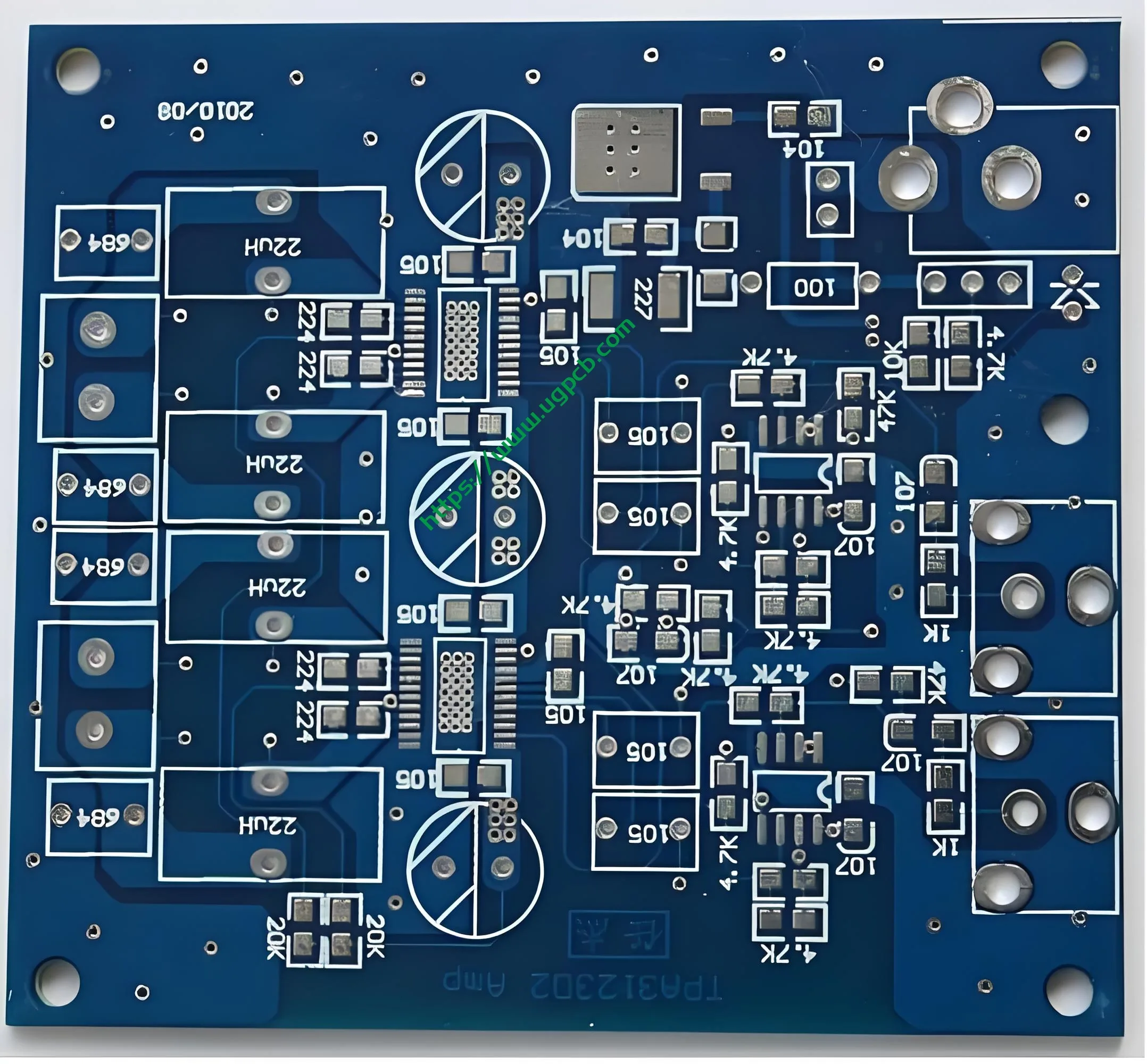
Структура двухсторонней печатной платы
Особенности печатных плат UGPCB:
-
Верхний и нижний медные слои: 35мкм толщиной, выгравированы в схемы.
-
Ядро FR-4: Изолирующая подложка толщиной 1,6 мм..
-
Покрытые сквозные отверстия: Металлизирован медью для соединения слоев.
-
Слоя припоя маски: Наносится на медь, исключая паяемые площадки.
-
Легенда шелкографии: Белая или черная маркировка для размещения компонентов..
Преимущества конструкции УГКПБ
-
Экономическая эффективность: Снижает материальные затраты на 30–50% по сравнению с многослойными альтернативами.
-
Повышенная гибкость дизайна: Поддерживает перекрестную маршрутизацию и оптимизированные схемы заземления..
-
Улучшенное управление температурным режимом: Сетчатые медные плоскости и тепловые переходы эффективно рассеивают тепло..
-
Высокая надежность: Отделка CTI600 и OSP продлить срок службы в тяжелых условиях.
Обзор производственного процесса
-
Подготовка материала: Разрезаем подложку FR-4 на панели размером 510x610 мм..
-
Бурение: Сверла с ЧПУ создают отверстия диаметром всего 0,2 мм для PTH. .
-
Химическое осаждение меди: Каталитическое окисление создает проводящий слой в отверстиях. .
-
Изображение шаблона: Фотолитография передает макеты схем с использованием УФ-воздействия..
-
Гальваника: Отложение меди приводит к утолщению дорожек и стенок отверстий до ≥20 мкм. .
-
Офорт: Удаляет нежелательную медь, определение следов.
-
Прикладная маска: Напечатаны и разработаны УФ-отверждаемые чернила.
-
ОСП-покрытие: Органический консервант, наносимый на открытую медь..
-
Шелкостная печать: Добавлены индикаторы компонентов.
-
Маршрутизация и V-скоринг: Панели разделены на отдельные доски.

Распространенные сценарии использования
-
Коммунальные подстанции: Реле защиты корпуса трансформаторов и фидеров.
-
Промышленные моторные приводы: Внедрение логики управления для предотвращения перегрузки.
-
Беспрерывные источники питания (UPS): Управление циклами зарядки/разрядки аккумулятора.
-
Умные счетчики: Включение мониторинга энергопотребления в режиме реального времени.

Заключение
Двусторонние печатные платы UGPCB для релейной защиты сочетают в себе современные материалы, точное машиностроение, и тщательное тестирование обеспечить непревзойденную надежность. С такими функциями, как Изоляция FR-4, ОСП-покрытие, и соответствие CTI600, они являются оптимальным выбором для критически важных энергосистем. Инженеры, стремящиеся повысить безопасность и долговечность оборудования, могут использовать опыт UGPCB для своего следующего проекта..


